Analysis of CIGS Thin Film PV
Home » Analysis of CIGS Thin Film PV
Cu(In,Ga)Se2 (CIGS) thin film PV is a thin film PV technology in its early stage of large scale commercialization. CIGS has the advantage of a high cell efficiency (approaching 20%) and module efficiency (~13%), a direct bandgap, a high absorption coefficient, and processes that can work for low cost, large scale manufacturing, including roll-to-roll substrates of polymer or stainless steel. The electronic properties of the cell are very tolerant to compositional variance of the Cu content. The CuInSe2 can be alloyed with Ga (common), Al and S to engineer the bandgap over a wide range for improved performance.
The main area for improvement of CIGS thin film PV is performance reliability and uniformity as manufacturing is scaled up.
Materials characterization using surface analysis methods can be used to support analysis of performance and R&D of efficiency improvements.
Figure 1 is a schematic of the CIGS Thin Film PV device structure shown above illustrates some of the ways surface analysis can help.

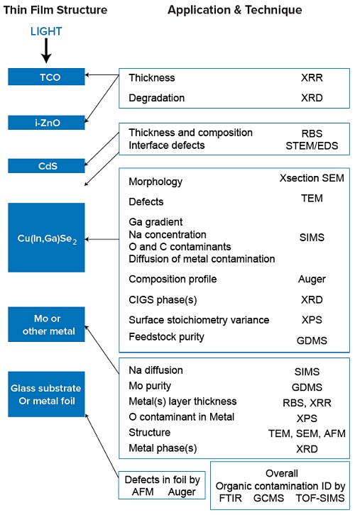
On the left side of the schematic we see the layered structure. The substrate in this case is soda lime glass, a source of needed Na in the device, but alternative substrates such as stainless steel foil or polyimide sheet are also used in which case an alternate method for adding Na is needed. In the schematic a metal (Mo in this case) is deposited on the glass substrate with thickness on the order of 0.5 µm. The CIGS layer is deposited next with thickness on the order of 2 µm and a thin (~50 nm) CdS layer is deposited on the surface of the CIGS. Alternatives to CdS include CdZnS, Zn(S, O, OH), ZnSe, ZnIn2Se4, In2S3, and ZnMgO.
Finally a Transparent Conductive Oxide (TCO) such as ZnO/ZnO:Al or ZnO/ITO of thickness 0.2 µm to 0.5 µm is deposited. The light enters from the TCO side, and is absorbed in the CIGS layer where electron-hole pairs are formed. The p/n junction at the CdS/CIGS heterojunction, or a homojunction formed by a Cd-doped surface region of the CIGS at the CdS interface, creates a depletion region which separates the electron and holes and allows them to be collected, thus generating the solar cell current. Two of the key steps in the CIGS solar cell design and fabrication are the process to introduce a controlled profile of the Ga in the CIGS layer and the process to introduce ~0.1% Na into the device. The CIGS layer must be Cu-deficient, and stability of the cell is attributed to a stable formation of a defect pair which is electrically inactive. Each of the layers is multi-crystalline.
On the right side of the schematic are shown some examples of materials analysis. Starting at the bottom, or the beginning of the cell formation, we have the metal layer on the glass substrate.
This metal layer is most commonly sputtered Mo which has a target resistivity and allows Na to diffuse from the glass substrate to the upper layers of CdS and CIGS. The thickness and micro-structure of the Mo film is critical to both resistivity and the ability to allow the Na to diffuse. Thickness can be measured by XRR. Microstructure can be characterized by XRD (phase ID), SEM, and AFM. Porosity can be characterized by TEM. Oxygen in the Mo film can affect the properties and this can be determined by XPS and RBS. SIMS can be used to profile the Na through the Mo into the upper layers. If the glass substrate is replaced by a metal foil such as stainless steel, defects in the foil can be characterized by AFM and Auger.
The CIGS layer deposited on the metal contact can be characterized by many techniques. Cross section SEM gives the grain and void morphology. TEM gives information on defects, including nanodomains. STEM/EDS provides information on fluctuations of the ratio of alloy components. SIMS gives the profile of the major constituents (Cu, In, Ga, Se) as well as impurities such as O and C contaminants and the desired Na. Auger can also profile the major constituents. XRD and GIXRD give CIGS phase ID, and XPS provides surface stoichiometry variance before the CdS layer is deposited.
Thickness and composition of the CdS layer can be obtained by XRR and RBS. The TCO layer composition and thickness can be determined by XRR and RBS while XRD can provide phase degradation under accelerated environmental aging tests.
In addition organic contamination that may enter the process at any step, including the module formation, can be determined by FTIR, GCMS, XPS, Raman, or TOF-SIMS.
Would you like to learn more about Analysis of CIGS Thin Film PV?
Contact us today for your analysis of CIGS thin film PV needs. Please complete the form below to have an EAG expert contact you.