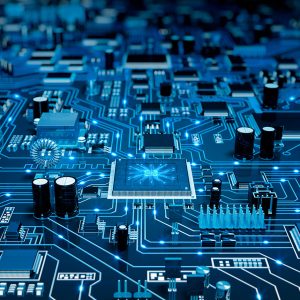
Exploring the Capabilities of Dual-Beam FIB-SEM

The dual-beam focused ion beam (FIB) – scanning electron microscope (SEM) is an advanced tool that combines precise sample milling/preparation with high-resolution imaging. It has two columns—one for FIB (usually using a gallium ion source) and one for SEM—allowing simultaneous milling and imaging of the sample. The FIB operates with nanometer precision, performing tasks like creating cross-sections, delayering samples, and generating thin, electron-transparent lamellae samples for TEM/STEM analysis. The SEM is crucial for locating areas for FIB milling, imaging the cross-section crafted by the FIB, and monitoring sample preparation progress. Both the FIB and the SEM use a highly focused beam (Ga ion and electrons, respectively) with energies from 1 to 30 keV to scan the sample and detect secondary or backscattered electrons generated. Secondary electrons provide insights into topography, while backscattered electrons offer information on the average atomic number. The FIB’s secondary electrons and ions can create images highlighting grain structure much better than the SEM due to strong channeling effects of Ga ions used in FIB. Additionally, both the FIB and the SEM can deposit metals or insulators on the sample for precise circuit editing. This dual-beam FIB-SEM is a versatile tool applicable to studying the surface and interior of various materials, including semiconductors, polymers, metals, and ceramics.

KWZ_0894-196

Using Dual Beam FIB-SEM for TEM Sample Preparation

The dual beam FIB-SEM can be used to prepare site specific Transmission Electron Microscopy (TEM) samples, crucial for resolving sub-nanometer features and achieving atomic resolution images. In TEM lift out sample preparation using the dual-beam instrument, the region of interest (ROI) undergoes meticulous steps in preparation for TEM analysis. Initially, the ROI is protected with an electron beam and/or ion beam-assisted deposited metal cap. The FIB is then utilized to create a trench around both sides of the ROI, cut free three sides of the ROI, and attach the sample lamella to a micromanipulator needle within the dual-beam system. Subsequently, the ROI is separated from the bulk sample, lifted out using the needle, and welded onto a TEM grid using ion-beam-assisted gas deposition. Afterward, the sample lamella is detached from the needle and securely affixed to the TEM grid. The final step involves thinning the sample to achieve electron transparency (less than 100 nm in thickness) for comprehensive TEM analysis.

KDW_0850-185

Dual-Beam FIB SEM at EAG

EAG has a network of more than 15 dual-beam systems, which include high-resolution field emission tools, tools for 300 mm wafer accommodation, plasma Focused Ion Beam (FIB) dual beams, and systems with Energy Dispersive Spectroscopy (EDS) detectors. In addition to our advanced hardware, we have a team of over 25 experts with diverse backgrounds, including Ph.D. ‘s, FAB process managers, and metallurgy specialists, who regularly work on dual beams. Our labs serve various industries such as semiconductor, medical devices, optics, energy storage, cell phones, piping, and printing. Contact us to learn how we can help you on your next project.

More content you might like...

To enable certain features and improve your experience with us, this site stores cookies on your computer. Please click Continue to provide your authorization and permanently remove this message.

To find out more, please see our privacy policy.