Quality of Metal Powder Feedstocks for AM Webinar
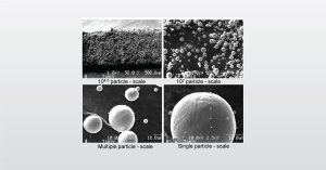
In this webinar we introduce Multiscale Assessment on the Quality of Metal Powder Feedstocks for Additive Manufacturing

In this webinar we introduce Multiscale Assessment on the Quality of Metal Powder Feedstocks for Additive Manufacturing
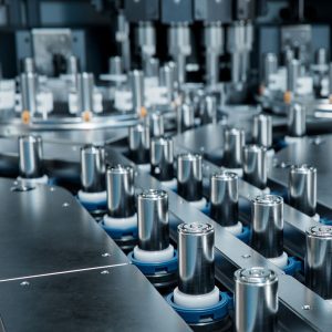
Measuring the chemical state of the battery components such as the cathode, anode, separator, electrolyte, contact layers and additives, at various stages of cycling, provides vital information about the electrochemical processes that occur during battery use.
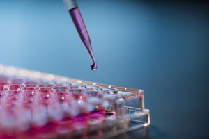
In vitro biocompatibility testing is a powerful tool in the risk assessment of wearable devices. View our webinar to learn more!
From semiconductor dopant profiling to contamination investigations, SIMS plays a critical role in solving some of the most demanding analytical challenges. Explore the applications where SIMS provides unique insights.
To enable certain features and improve your experience with us, this site stores cookies on your computer. Please click Continue to provide your authorization and permanently remove this message.
To find out more, please see our privacy policy.