Ask the Expert: Is Your Wearable Device Safe?
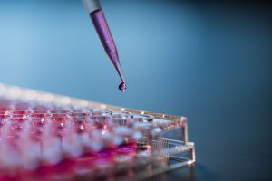
In vitro biocompatibility testing is a powerful tool in the risk assessment of wearable devices. View our webinar to learn more!
In vitro biocompatibility testing is a powerful tool in the risk assessment of wearable devices. View our webinar to learn more!
Solids fall under two main categories: amorphous and crystalline. These two types of solids have different properties that may be more beneficial for certain products or applications.

The roughness of a surface and how it interacts with surrounding materials and elements can have a significant impact on material technology and its functionality.
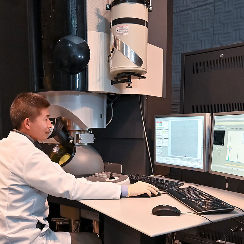
This webinar will introduce you to AFM and OP, with a overview of the theory of each technique and representative examples of them in action.
To enable certain features and improve your experience with us, this site stores cookies on your computer. Please click Continue to provide your authorization and permanently remove this message.
To find out more, please see our privacy policy.