Surface Analysis of α-Si, µc-Si Thin Film PVα-Si, µc-Si Thin Film PV
Home » Surface Analysis of α-Si, µc-Si Thin Film PV
Amorphous Si (α-Si), microcrystalline Si (µc-Si), nanocrystalline Si (nc-Si), amorphous SiGe (α-SiGe), and microcrystalline SiC (µc-SiC), all with H, are thin film materials that can make up thin film PV stacks ranging from simple α-Si thin film to more complex tandem and multi-junction thin film. α-Si has been one of the oldest thin film PV commercial technologies, but with relatively low cell efficiency after light-induced degradation. The addition of the other thin film materials are intended to increase the efficiency by converting more of the sun’s spectrum and by reducing the light-induced degradation.
The main areas of improvement are stable efficiency increases towards 10%, and scale up to reliable and uniform large scale manufacturing.
The schematic of the α-Si thin film PV (generic name for all the combined films) illustrates some of the ways surface analysis can help.
On the left side of the schematic we see a composite of various layered structures. Light enters from the top through a glass cover and passes through a Transparent Conducting Oxide (TCO) SnOx:F, ZnO:Al or ZnO:B. The light is then absorbed in the various layers of α-Si:H, µc-Si:H, nc-Si:H, α-SiGe:H, µc-SiC:H, depending upon the cell design; doping to form the p-n junction(s) is done by adding B or P in the deposition processes.
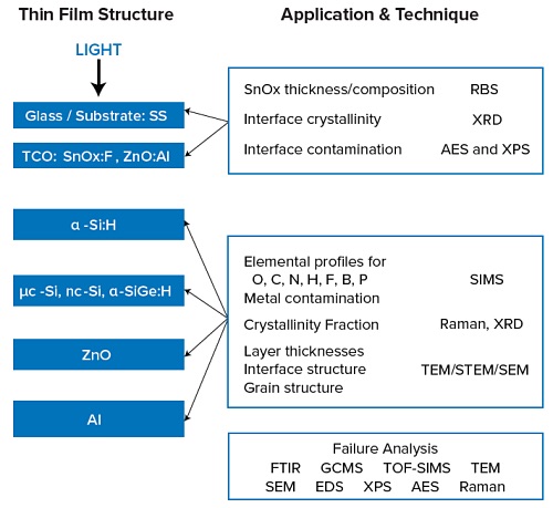
Below the absorber layers there is another TCO followed by a backside contact such as Ag or Al. This is all supported on a substrate which may be stainless steel foil, polyimide, or glass. The entire stack (apart from the glass) is a few microns thick.
On the right side of the schematic we see some example applications of surface analysis techniques. Thickness and composition of the upper TCO can be characterized by RBS, XRR or XPS, crystallinity and phases by XRD, and contamination between the TCO and first α-Si:H layer by XPS or AES. Elemental profiles of atmospherics (O, C, N, H), dopants (B, P) and F as well as metal contamination can be profiled by SIMS. Crystallinity fraction in the absorber layers can be determined by Raman or XRD. Layer thicknesses, interface structure and grain structure can be determined by TEM, STEM and SEM for the absorber layers, the lower TCO and metal contact. Failure analysis can be supported by FTIR, GCMS, TOF-SIMS, TEM, STEM/EDS, SEM, EDS, XPS, AES and Raman.
Would you like to learn more about analysis of α-Si, µc-Si Thin Film PV?
Contact us today for your analysis of α-Si, µc-Si Thin Film PV needs. Please complete the form below to have an EAG expert contact you.