A TEM-based Materials Analysis Study into 22nm FinFET Technology
Home » A TEM-based Materials Analysis Study into 22nm FinFET Technology
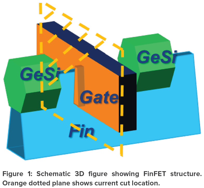
Fin field-effect-transistor (FinFET) is the basis for modern nanoelectronic semiconductor device fabrication. Figure 1 schematically shows its 3D structure design. The gate wraps around the channel on the raised Silicon fin, in which charge current flows between SiGe source and drain. Compared to traditional planar transistors, FinFET provides greater surface area between gate and channel and thus better control of the electric field and leakage reduction in the “off” state [1].
In this application note, we present a study into the structure, elemental distribution and crystal orientation of a 22nm FinFET structure, using Nanolab Technologies’ state-of-art TEM instruments and other TEM-based analysis techniques including EELS and PED.
TEM lamella of ~50 nm thickness was prepared at Fin location as labeled in figure 1, by in-situ FIB lift-out technique.
Download the App Note for more information on the study of 22nm FinFET technology
Would you like to learn more about analysis of 22nm FinFET's?
Contact us today for your 22nm FinFET analysis needs. Please complete the form below to have an EAG expert contact you.