Determining Density of Thin Films
Home » Determining Density of Thin Films
Thin films are widely used in many high-tech devices and consumer products. The reason for their use varies widely but is predominantly due to their physical, mechanical, electrical, thermal or decorative properties.
The quality and consistency of these films is of great interest to manufacturers and users of these materials. One of the key film properties of interest is density. This paper addresses the processes best used to measure the density of such films. The elemental composition and film thickness can also be determined and are also discussed.
The use of X-ray Fluorescence Spectroscopy (XRF) to determine film thickness and composition is coupled with Rutherford Back Scattering Spectrometry (RBS) which determines the film’s areal density and elemental composition. The third technique of interest is Dual Beam Focused Ion Beam (DB FIB) which can directly measure film thickness. These techniques combine to provide the film’s elemental composition, thickness and density.
Sample Preparation
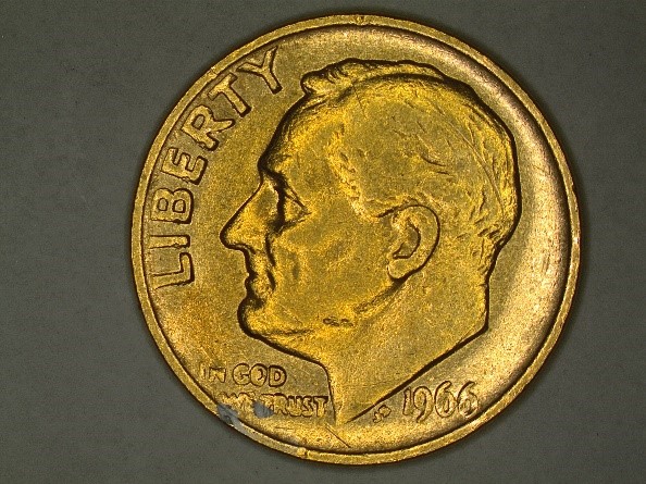
The sample we used in this study is a US 10 cent coin that was coated with a thin layer of gold. This film is used for demonstration purposes only and is not as uniform as state-of-the-art films used for demanding electronic or semiconductor applications, but it is a good example for the techniques and measurements that can be made on real films and film stacks. No sample preparation was required for any of the techniques.
XRF measurements were made on both sides of the coin at several locations. The RBS measurement and the DB FIB cross section were made in one location only.
Information Obtained
Optical microscopy allows inspection of devices for major defects such as large cracks, discolorations, and gross contamination. It is often used to document the samples prior to analysis. Bright field and dark field or a mix can be used to examine and document specific surface features of different types, e.g. pits, scratches or particles.
XRF uses X-rays to excite fluorescence in materials. The wavelength of the fluorescence shows the species present in the sample and the intensity of the fluorescence can be used to determine the elemental composition. Layer thicknesses can also be determined on flat samples. Detection limits are typically in the PPM (parts per million) range for most elements, but this varies with atomic number.
In Rutherford Back Scattering Spectrometry (RBS) MeV alpha particles (He nuclei) bombard the sample and the energy of the scattered ions are measured. The data obtained are modeled to determine the elemental composition and layer structure. The areal density of the film can also be determined. With this technique, if the film thickness is known, then the density can be determined and vice versa: if the density is known, then the film thickness can be calculated.
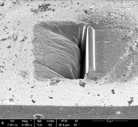
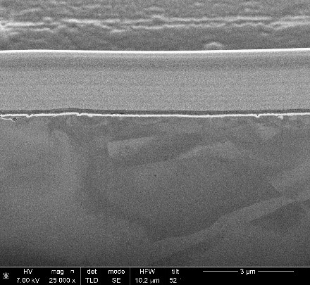
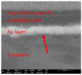
Dual Beam FIB can be used to cross section through the thin film layers to directly measure the film thickness(es) using subsequent in situ SEM inspection. The interface and the entire film can also be imaged to investigate the sharpness of the interface and to determine if any voids/defects are present. DB FIB cross-sections can be made at any accessible location on a sample.
| Method | Information Acquired | Comments |
| Optical microscopy | Color images of sample, dimensional measurements. | Limited to ~ 2500×. Only detects visible light. |
| WDXRF | Elemental composition and film thickness | Minimum sampling area is 0.5 mm diameter PPM detection limits |
| RBS | Elemental composition up to 2 microns depth. Elemental areal density and calculated film thickness. | No standards required. |
| DB FIB | Allows direct imaging of a cross section of the sample. Grey scale images with high depth of field with magnifications up to 100,000× on standard tools. | Small area cut. Only shows that one plane in the sample. Limited depth of approximately 50 microns. |
Table 1. Test Matrix
Results of Each Test
Optical imaging in this case was used just to document the sample and inspect it prior to analysis.
XRF is used to detect the elements present in the film and also in the underlying substrate, with ppm detection limits. With this data and knowing the gold is in the overlying film, calculations can be made to determine the thickness of the film. Several locations were analyzed to determine the overall uniformity of the gold coating.
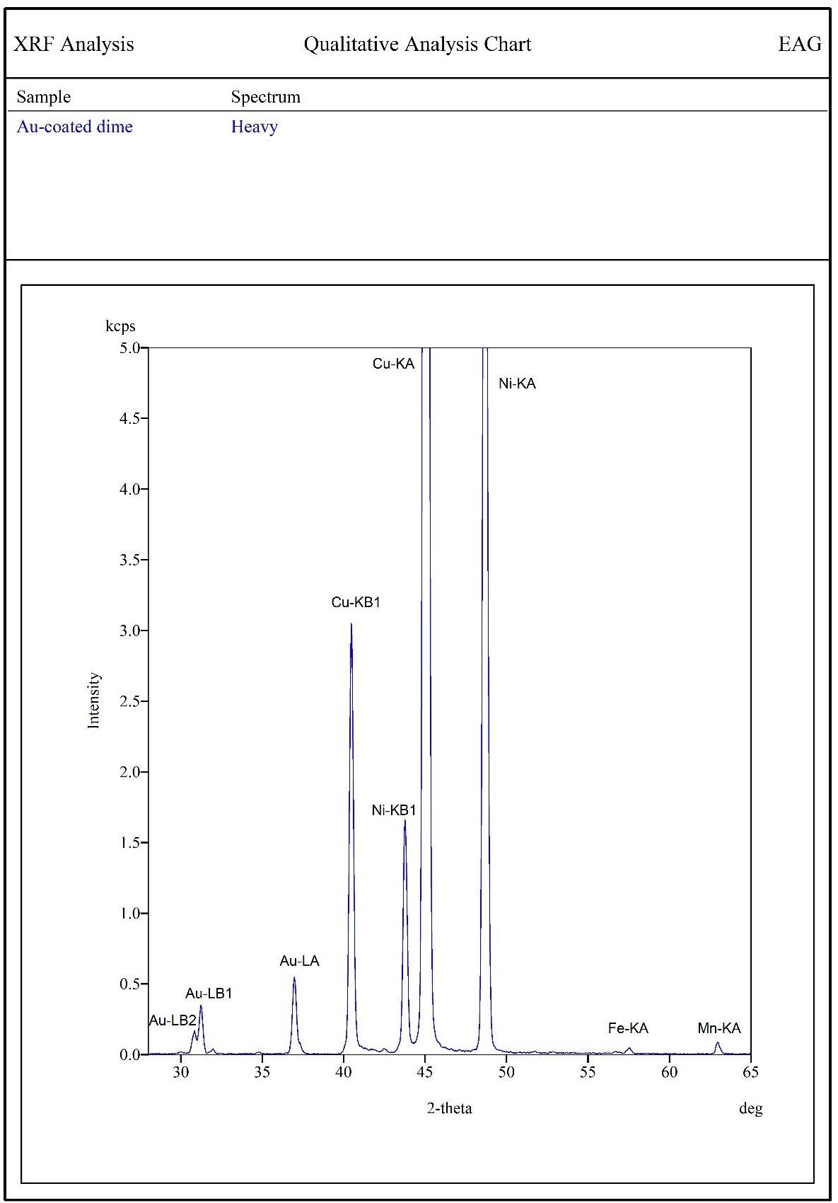
Table 2. Gold coating (front side)
| Element | Coating (wt%) | Substrate (wt%) |
| Au | 100 | |
| Cu | 73.9 | |
| Ni | 25.7 | |
| Co | 0.019 | |
| Fe | 0.059 | |
| Mn | 0.30 | |
| Zn | 0.042 |
Table 3. Elemental composition of the surface layer and the substrate, the coating is pure Au.
| Film | Substrate | Substrate | |||
| Au | Cu | Ni | |||
| nm | St. Dev. | RSD (%) | wt% | wt% | |
| Spot 1 | 98 | 0.29 | 0.30 | 75.4 | 24.6 |
| Spot 2 | 87 | 0.49 | 0.56 | 75.1 | 24.9 |
| Spot 3 | 112 | 0.33 | 0.29 | 75.2 | 24.8 |
The coating thickness is nonuniform. Each analysis was repeated 3 times at each location (note the RSD determined from the repeat measurements). WDXRF has excellent precision and can measure sub-nm scale differences in thickness.
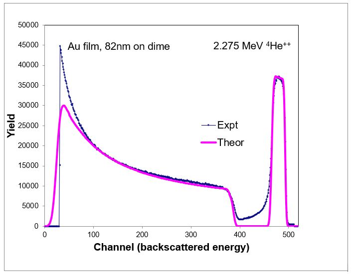
Table 5. RBS elemental composition, showing an aerial density of 4.85e17 atoms/cm2
| RBS Thickness [nm] | Atomic Concentrations [at%] | Assumed Density [at/cc] | ||||
| Ni | Cu | Au | ||||
| Layer 1 | 82 | – | – | 100 | 5.90E22 | |
| BULK | – | 26.5 | 73.5 | – | 8.63E22 | |
The average thickness for this film was measured to be 70 nm by Dual Beam FIB. The film is rough with a standard deviation of 8 nm, as measured directly using the SEM mounted on the DB FIB.
The density of the gold film can be calculated using the areal density obtained from RBS and the layer thicknesses from either XRF or DB FIB. The XRF gives an average thickness over a larger area while the DB FIB shows the film thickness and variation in a much smaller specific location.
Using the atomic mass of gold, 3.2707×10⁻²² g/atom, this results in a range of 22.6-24.0 g/cm3 which compared to the common density of gold of 19.3 g/cm3 (see table below).
| Aerial density (atom/cm2) | Thickness | Atom Density (atm/cm3) | Calculated Density g/cm3 |
| 4.85×10¹⁷ | 70-87 nm | 6.91 X10²² | 22.6-24.0 |
Summary
The use of thin films in products requires a knowledge of the film properties. This paper illustrates a procedure to determine the composition, thickness and density of a film. The three techniques used on different locations on the sample provide a range of thicknesses. This sample was checked and the gold coating thickness was found to be variable. The analyses of the techniques were repeated and the individual locations provide repeatable results however the sample variation across the analyzed regions shows the non-uniformity of the coating.
While there are alternative techniques to determine film thickness and composition this approach has the advantages of direct measurement of the thickness (via DB-FIB) at a particular location and elemental composition determination with excellent detection limits (via XRF) along with averaged thickness over a larger area. The RBS then adds the capability to measure the aerial density and ultimately provide a film density. This combination of techniques enables average thickness and specific area measurements to better understand the thickness variations in the film(s).
Additional properties of thin films can be investigated with other techniques: roughness with AFM, Stress and texture by XRD, trace contaminations with SIMS, grain structure with EBSD and surface composition with XPS or Auger Electron Spectroscopy.
Would you like to learn more about Determining Density of Thin Films?
Contact us today for your determining density of thin film needs. Please complete the form below to have an EAG expert contact you.