High Resolution X-ray Diffraction (HR-XRD) Measurement of Compound Semiconductors
Home » High Resolution X-ray Diffraction (HR-XRD) Measurement of Compound Semiconductors
High resolution XRD (HR-XRD) is a well known method for measuring the composition and thickness of compound semiconductors such as SiGe, AlGaAs, InGaAs, and other materials.
When dopants or impurities are added substitutionally to a single crystal lattice the lattice will be strained by the presence of the dopant atoms. For example, in the case of a Si lattice, the presence of Ge atoms in the lattice results in compressive strain since the Ge atoms are larger than the Si atoms in the lattice. This strain changes the spacing of the Si lattice, and this difference in spacing can be detected by HR-XRD.
DISCUSSION
Shown in Figure 1 is a theoretical HR-XRD scan from a generic structure with compressive strain, such as a 10nm SiGe layer on Si. The sharp peak at 0 degrees is from the Si lattice in the substrate.
The presence of the larger Ge atoms causes the Si atoms in the SiGe layer to be spaced further apart, shifting the diffraction peak to lower angles (to the left of the substrate peak). The diffraction peak from the SiGe layer is much broader than the diffraction peak from the Si substrate because of the thinness of the 10nm SiGe layer.
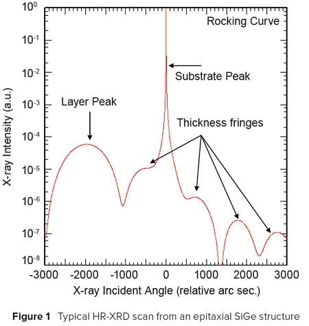
In such a thin layer there are only a few rows of aligned atoms available to generate a diffracted signal, so the x-rays are diffracted over a (relatively) wide angle compared to diffraction from the Si substrate where there are thousands of rows available to generate the diffracted signal. If the structure was under tensile strain then the Si atoms would be spaced closer together than those in the substrate and the layer peak would be shifted to the right of the substrate peak. The additional peaks, called “thickness fringes” are from constructive interference from X-rays reflected from the interface between the SiGe layer and the Si substrate. This is the same signal that is used for X-ray Reflectivity (XRR) analysis, and can be used to determine the thickness of the strained layer.
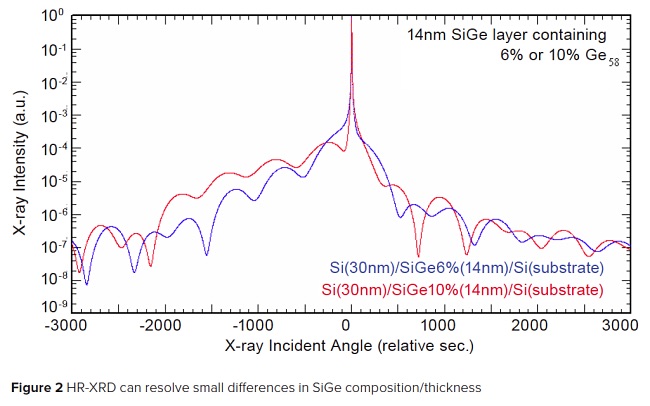
This method can be used to determine the composition of strained layers. Shown in Figure 2 are theoretical HR-XRD scans from two samples consisting of 30nm of Si on 14nm of SiGe on Si. In one case there is 6% Ge in the lattice, while in the other case there is 10% Ge. HR-XRD can easily resolve the difference between these two structures as well as determine the thickness of the layer from the thickness fringes.
Furthermore, advanced modeling can provide accurate descriptions of features such as graded SiGe layers. A wide variety of epitaxial materials can be measured with HR-XRD, such as AlGaAs, InGaAs, InGaN, etc. Typically XRD can determine the composition of such layers to within 1 atom%, however, it should be noted that HR-XRD assumes that all of the dopant is present in the lattice.
If dopants or impurities are interstitial in nature then they will not be detected by HR-XRD as they have no effect on the lattice spacing. Also, HR-XRD does not actually identify the dopant, so it should be used only for the measurement of known structures, not to identify unknown species in these structures.
Would you like to learn more about Measurement of Compound Semiconductors?
Contact us today for your measurement of compound semiconductor needs. Please complete the form below to have an EAG expert contact you.