Rapid Threading Dislocation Typing in GaN Using STEM
Home » Rapid Threading Dislocation Typing in GaN Using STEM
STEM provides images of dislocations with greatly simplified contrast, allowing rapid dislocation typing in both cross section and plan view samples.
Compound semiconductor GaN and its alloys have wide applications in electronic and opto-electronic devices such as light emitting diodes and laser diodes. However, the lack of lattice-matched substrates from its growth results in high density of vertical threading dislocations (VTDs).
Research has shown that the VTD type (edge, screw, or mixed) has a strong influence on the device performance. As such, there is a strong need to effectively determine VTD type and density.
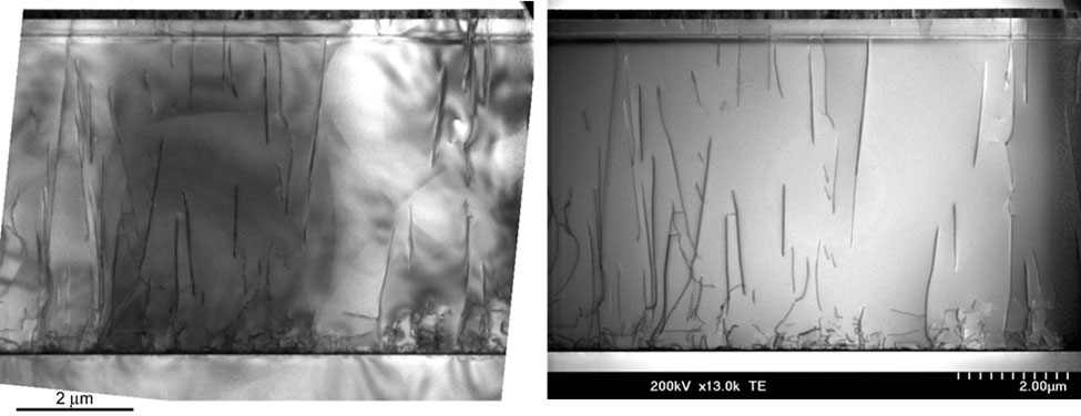
Figure 1: Comparison of VTD in GaN imaged with conventional TEM bright field (left) and STEM bright field (right)
Traditionally, dislocation typing in various materials is carried out by extensive conventional transmission electron microscopy (TEM) analysis of cross-section samples. However, TEM images are complicated by thickness fringes and bend contours as is shown in the left image in Figure 1.
A corresponding scanning transmission electron microscope (STEM) image from the same cross section sample is shown in the right side. As compared to the TEM, the scanning convergent electron beam of the STEM provides images of dislocations with greatly simplified contrast, allowing rapid observation of all dislocation types simultaneously.
Would you like to learn more about Rapid Threading Dislocation Typing in GaN?
Contact us today for your rapid threading dislocation typing in GaN needs. Please complete the form below to have an EAG expert contact you.
To enable certain features and improve your experience with us, this site stores cookies on your computer.
Please click Continue to provide your authorization and permanently remove this message.