Silicon Carbide is a very important material for high-power, high-temperature, high-frequency and high-radiation devices due to its superior electronic and thermal properties. Dramatic progress in SiC-based power transistors, LEDs, and sensors have made it imperative to accurately control dopant and impurity levels.
Secondary Ion Mass Spectrometry (SIMS) has very high detection sensitivity for a variety of elements. Its unique profiling capability can provide quick and precise feedback in dopant level, junction depth, and impurity distribution in SiC sample, including patterned device structures. It is an essential tool for process control and problem solving in wafer growth and device manufacturing.
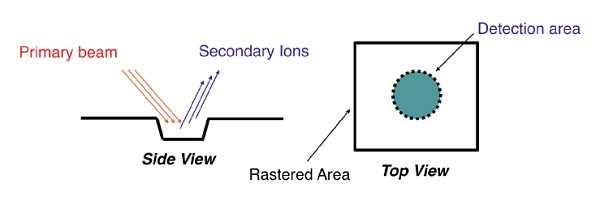
Either oxygen (O2+) or cesium (Cs+) primary ion beams are used for SIMS analysis. The spot size of a focused primary ion beam is typically 2 to 20 μm. This primary beam is rastered over a square area, usually on the scale of up to several hundred microns on a side.
Detection of Secondary Ions
Secondary ions generated from the central portion of the rastered area are measured after being mass separated in a mass spectrometer. In magnetic sector SIMS instruments secondary ions can be detected using electron multipliers, Faraday cups or ion imaging detectors.
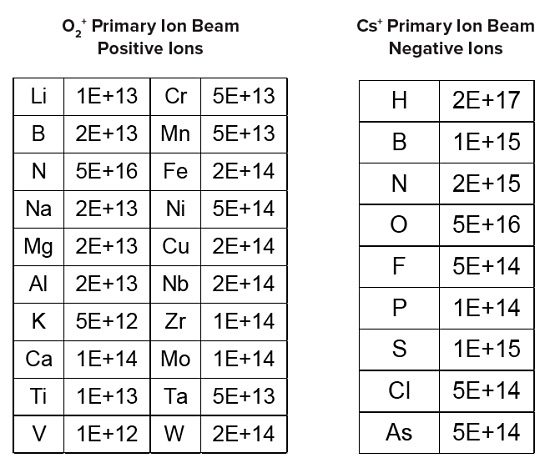
SIMS DETECTION LIMITS (at/cm3) IN DEPTH PROFILING MODE*
*Detection limits in semi-bulk or bulk mode may be significantly lower than those obtained in depth profiling mode.
QUANTIFICATION OF SiC
Concentration Calibration
Concentrations are calibrated based on ion implant standards into clean SiC.
Depth Calibration
The acquisition time of a depth profile is converted to depth using the measured analytical crater depth (using a stylus profilometer).
IMPROVEMENT OF SIMS DETECTION LIMITS IN SiC
Improvement of detection limits of N
Improved vacuum and a modified Cs+ source that provides high beam current density, has led to improved detection limits for N.
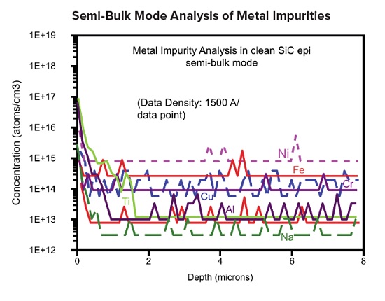
Improvement of detection limits for B, Al, and other metal elements
The instrument used is limited to the measurement of Si, C, and SiC material to reduce potential contamination from other materials. A larger Field Aperture and a non-standard Contrast Diaphragm are used to increase the detection area and collection angle, thus increasing our sensitivity for these elements.
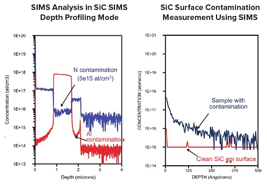
Detection limits under profiling condition in SiC
N: 2-5E15 atoms/cm3
B: 2E13 atoms/cm3
Al: 2E13 atoms/cm3
TYPICAL SiC ANALYSES
Depth profiling of dopants and impurities, including in small devices
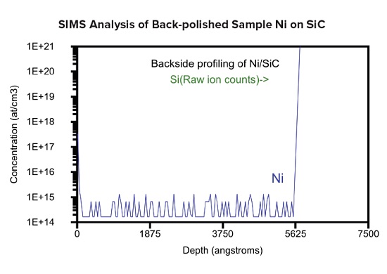
SIMS analysis with sample polishing to access deeper or buried layers (frontside or backside)
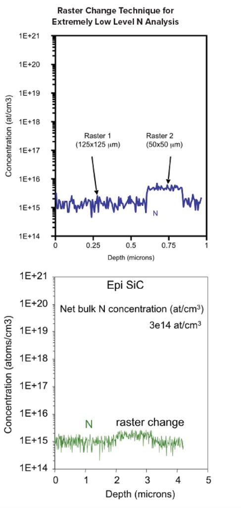
Extremely low concentration nitrogen analysis
SiO2/SiC interface analysis
Raster change during N profile. The N shown is quantified for the 50×50μm raster
RASTER CHANGE TECHNIQUE FOR LOW N CONCENTRATION MEASUREMENT
The “raster change” method provides an accurate way to determine and remove the contribution of background nitrogen to the measured signal, because both nitrogen and matrix ion intensities can be analyzed at the same location of the sample by changing the primary ion beam raster size during a profile.
In this technique, the sample is initially sputtered by the primary beam using a large raster. After the profile reaches a constant level, the primary raster size is reduced, while the collection area for secondary ions stays the same. This increases the current density of primary ions within the collection area.
A disadvantage of this technique is that it can be used only on uniformly doped samples or in a thick enough layer that concentration is uniform.
SiC 4-INCH WHOLE WAFER ANALYSIS
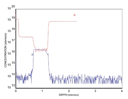
SIMS profile of Al and N from a 2” SiC wafer. The Al profile was acquired using oxygen beam sputtering, and N profile was acquired using Cs beam sputtering. The whole wafer capability provides doping concentration and thickness of each epi layer without breaking the wafer. A N detection limit of ~2e16 atoms/cc can be achieved after ~2 hours of pumping.
Modified Cameca 4f with 4” Sample Intro System
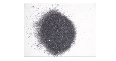
SIMS ANALYSIS OF INDIVIDUAL SiC PARTICLES FOR ACCURATE BULK CONCENTRATION MEASUREMENT
Using a special sample preparation technique and a new SIMS analytical protocol, individual SiC particles with a size ranging from 100 μm to 500 μm in a SiC powder sample can be analyzed. This innovative approach eliminates contributions from surface contamination to bulk concentration.
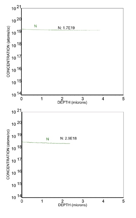
N profiles for two different SiC particles from the same batch of powder samples. The SIMS results for these two particles show good batch bulk concentration consistency.
Would you like to learn more about SIMS Measurements of Silicon Carbide?
Contact us today for your SIMS Measurements of Silicon Carbide needs. Please complete the form below to have an EAG expert contact you.
To enable certain features and improve your experience with us, this site stores cookies on your computer.
Please click Continue to provide your authorization and permanently remove this message.