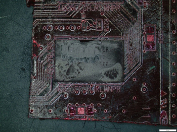
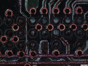
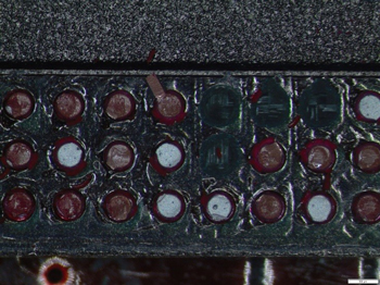
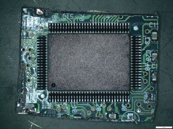
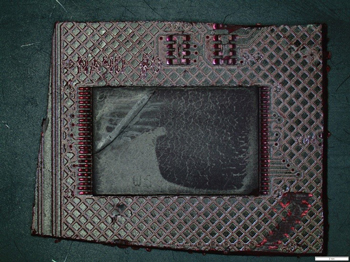
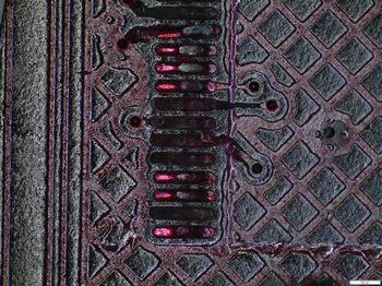
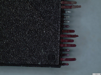
Dye and Pry involves cleaning a sample to remove debris and flux around solder, then exposing it to a red dye by immersion. The sample is then exposed to either vacuum or pressure to ensure the dye penetrates into all cracks, separations and surfaces with exposure to the outside of the device.
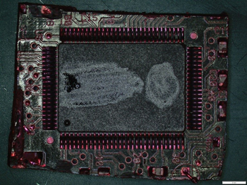
The parts are then baked in an oven until fully dry. The ink must be fully dried to avoid smearing later. The device is then separated by prying or flexing of the PCB. The interfaces now separated are inspected optically. Failure sites are imaged and identified.
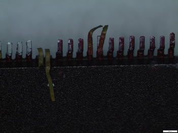
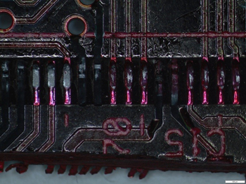
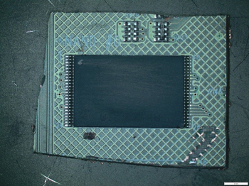
For PQFPs and TSOPs on a PCB the areas of interest are the lead fingers. The ink gets in where there are cracks in the solder or failure to reflow the solder. These are areas of weak bonding and likely reliability failures. The silver colored areas are where the ink was unable to ingress showing good bonding.
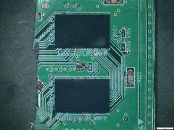
Dye and Pry is an excellent way to inspect a large number of bonds (leads, solder ball, seals..) at one time.
Contact us today for your dye & pry needs. Please complete the form below to have an EAG expert contact you.
To enable certain features and improve your experience with us, this site stores cookies on your computer.
Please click Continue to provide your authorization and permanently remove this message.