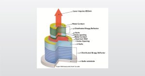
Ion-Exchanged Glass: Smart Technology for Smartphones
Ion-exchanged glass is used in a variety of applications where strength, durability, and resistance to damage are important. Applications like smartphone screens.
Home » Analyzing Red LEDs with PCOR-SIMS
Televisions, computer screens, cell phone screens etc. are getting clearer, sharper, brighter and use much less power. This is all possible through LEDs – or light-emitting diodes. LED display applications range from our smartwatches to large advertising billboards. They also have a longer lifespan than traditional lighting technology.
An LED is a semiconductor device, which can emit light when an electric current passes through it. To do this, holes from p-type semiconductors recombine with electrons from n-type semiconductors to produce light. Inside the semiconductor material of an LED, the electrons and holes are contained within the energy bands. The separation of these bands (i.e., the bandgap) determines the energy of the photons (light particles) that are emitted by the LED. The photon energy determines the wavelength of the emitted light, and hence its color. Different semiconductor materials with different bandgaps produce different colors of light. The color can be fine-tuned by altering the composition of the light-emitting or active, region.1
Until the mid-90s LEDs had a limited range of colors. With the development of LEDs based on the gallium nitride (GaN) material system the expanded color palette resulted in many new applications. Typical blue and green LEDs are gallium nitride based, but the red LED is made up of GaP (gallium phosphide), InAlP (indium aluminum phosphide), InAlGaP (indium aluminum gallium phosphide), InGaP (indium gallium phosphide), AlGaAs (aluminum gallium arsenide), GaAs (gallium arsenide). Red LEDs are frequently promoted in skin treatments as experts believe that red LED light acts on cells in the skin known as fibroblasts, which play a role in the production of collagen.2
When analyzing red LEDs, the scientists at Eurofins EAG Laboratories (EAG) utilize PCOR-SIMSSM. PCOR-SIMSSM is a point-by-point data correction algorithm, which uses the alloy composition at a given data point for proper calibration of Secondary Ion Mass Spectrometry (SIMS) intensities. This corrects for matrix effects therefore layer thicknesses and elemental concentrations are determined more accurately.
With over 40+ years of experience, EAG is an expert in SIMS. In fact, EAG is the world leader in commercial SIMS analysis – and has been for decades. The depth and scope of experience and commitment to research and development in the SIMS field is unrivaled. At EAG there is a long history of working with customers as partners. EAG helps its customers with challenges prior to going to final production or final product fabrication. Understanding manufacturing, EAG is equipped to solve complex problems that may arise in trials and much more.
Contact EAG today to learn more about our depth of knowledge and experience and how PCOR-SIMSSM is the best choice for analysis of red LEDs.
1“What is an LED?” 1 September 2004. LEDs Magazine. 8 June 2022. <https://www.ledsmagazine.com/leds-ssl-design/materials/article/16701292/what-is-an-led>
2“Diseases & Conditions.” 1 October 2019. Harvard Health Publishing. Article. 6 June 2022. <https://www.health.harvard.edu/diseases-and-conditions/led-lights-are-they-a-cure-for-your-skin-woes>.
Ion-exchanged glass is used in a variety of applications where strength, durability, and resistance to damage are important. Applications like smartphone screens.
In this webinar we introduce failure analysis of ICs and other components in the product development cycle and for improving current products
Cryo TEM involves performing TEM analysis while keeping the sample at cryogenic temperatures, around -170°C.
February 12, 2025
During this live Ask the Expert event, we will answer pre-submitted questions from our audience regarding Silicon Carbide for High Powered Electronics. EAG Laboratories has a vast depth of experience analyzing silicon carbide using both bulk and spatially resolved analytic techniques and is the world-leading materials characterization and engineering resource for semiconductor testing.
To enable certain features and improve your experience with us, this site stores cookies on your computer. Please click Continue to provide your authorization and permanently remove this message.
To find out more, please see our privacy policy.