A Solution for Sensitive Materials – Cryo FIB
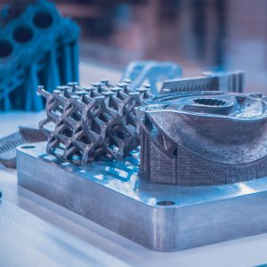
Cryo FIB uses a cold sample stage that can be controlled to -135°C making it it more suitable for temperature sensitive materials.
Home » Nanoprobing in the Evolving World of Electronic Systems
In the changing world of electronic systems, where devices are getting smaller and more complex, failures can lead to costly downtime, delays, recalls, and damage to reputation. It’s crucial to proactively find and fix these issues, primarily as devices use advanced materials and processes. A comprehensive approach to analyzing electronic system failures is essential. Nanoprobing becomes crucial for understanding advanced semiconductor devices, finding faults, and conducting thorough failure analysis. Its importance also extends to advancing and ensuring the quality of electronics and other semiconductor technologies.
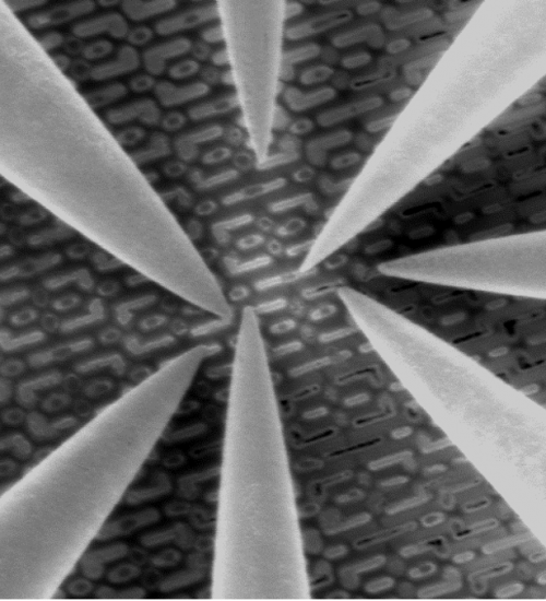
Nanoprobing is a highly specialized and precise analytical technique in semiconductor physics and electronics. It involves using nanometer-scale probes to make electrical contact with, manipulate, and measure the electrical properties of individual nanoscale structures within semiconductor devices. It is crucial for the electronics and semiconductor industries as it enables precise and non-destructive analysis of nanoscale structures and devices. It aids in quality control, failure analysis, design validation, and scientific research, contributing to developing more reliable and advanced electronic devices and materials.
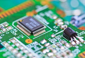
Nanoprobing is a vital method for analyzing and testing electronic materials, and it can be applied to a broad range of components such as integrated circuits, transistors, diodes, microprocessors, CPUs, and printed circuit boards. This comprehensive approach extends to other electronic elements and materials, making nanoprobing an indispensable tool in electronic analysis, fault localization, and testing.
We are delighted to introduce our state-of-the-art nanoprobing capabilities, featuring cutting-edge Kleindiek equipment. This innovative system empowers us to conduct precise measurements and thorough failure analysis of advanced nodes, delivering detailed and highly accurate information to our customers. By harnessing this technology, we ensure our clients stay at the forefront of semiconductor technology development, guaranteeing the reliability and performance of their products.
Our system addresses sub-10 nanometer structures on samples up to 20 x 20 millimeters, with a voltage range of +/- 100 V for DC measurements (+/- 50 V for current imaging). Furthermore, a heating & cooling insert enables device characterization over an extended temperature range between -20ºC – +150ºC. EBAC, EBIC, and EBIRCH imaging capabilities are available for fault isolation.
Nanoprobing plays a critical role in comprehending and evaluating the performance of advanced semiconductor devices, detecting faults, and conducting failure analysis. Its significance extends to the advancement and quality assurance of electronics and other semiconductor technologies. For further information, contact us today.

Cryo FIB uses a cold sample stage that can be controlled to -135°C making it it more suitable for temperature sensitive materials.
Contamination control and defect reduction are critical issues in the manufacturing process of compound semiconductor devices which can impact the performance of the end product. We can provide valuable insights to identify contaminants and characterize materials throughout the product lifecycle.

Damage caused by ESD is one of the primary failure mechanisms for integrated circuits. Testing susceptibility to ESD events is crucial in the success of electronic devices and is essential for the qualification process.

Solid-state batteries are redefining energy storage. Learn about the five families of solid-state electrolytes (SSEs) and how Eurofins EAG Laboratories provides advanced materials and interface analysis to support the next generation of battery analysis.
To enable certain features and improve your experience with us, this site stores cookies on your computer. Please click Continue to provide your authorization and permanently remove this message.
To find out more, please see our privacy policy.