XRF Webinar
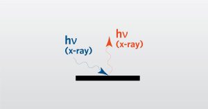
In this webinar we introduce X-ray Fluorescence Spectroscopy (XRF) which is a analytical technique used for elemental analysis of materials.


In this webinar we introduce X-ray Fluorescence Spectroscopy (XRF) which is a analytical technique used for elemental analysis of materials.
October 23
During this live Ask the Expert event, we will answer pre-submitted questions from our audience regarding brazing.
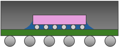
Automated Test Equipment (ATE) systems are carefully designed to test a wide range of semiconductor devices. EAG provides tailored ATE test solutions to meet the unique needs of clients.
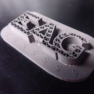
GC-MS can help with failure analysis or contamination characterization analysis on 3D printed parts. Utilizing a variety of different sampling techniques, GC-MS is a versatile tool that can identify specific species of volatile organic compounds.
To enable certain features and improve your experience with us, this site stores cookies on your computer. Please click Continue to provide your authorization and permanently remove this message.
To find out more, please see our privacy policy.