EAG Discovery Lunch, Sunnyvale | In-Person Networking Event
Join us for an engaging in-person event at our Sunnyvale CA lab.
Join us for an engaging in-person event at our Sunnyvale CA lab.
ATE testing automates and streamlines the testing process of microelectronic devices by using specialized hardware and software to perform a wide range of functional tests under various conditions. Come learn more about ATE and what EAG can do for you.
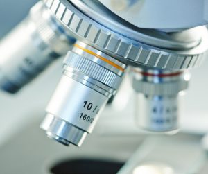
LA-ICP-MS is a technique that uses direct micro-scale sampling to provide high precision elemental characterization of solid materials.
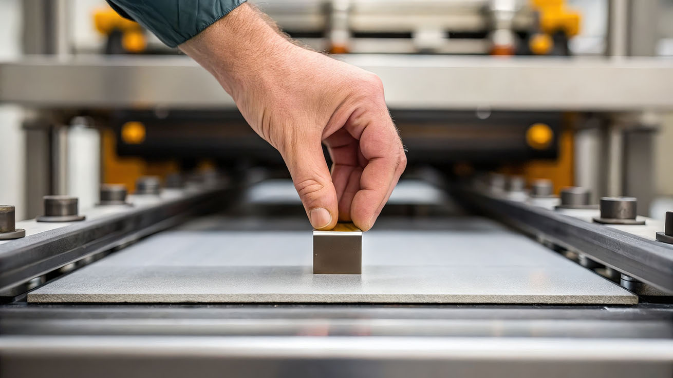
Rare earth magnets power some of today’s most advanced technologies. Part 3 of this series explores how the magnets are produced, challenges of maintaining purity at every step, and why precision analysis is essential for building a reliable supply chain.
To enable certain features and improve your experience with us, this site stores cookies on your computer. Please click Continue to provide your authorization and permanently remove this message.
To find out more, please see our privacy policy.