
4th Frontiers in Electron and Scanning Probe Microscopy for the Physical and Life Sciences

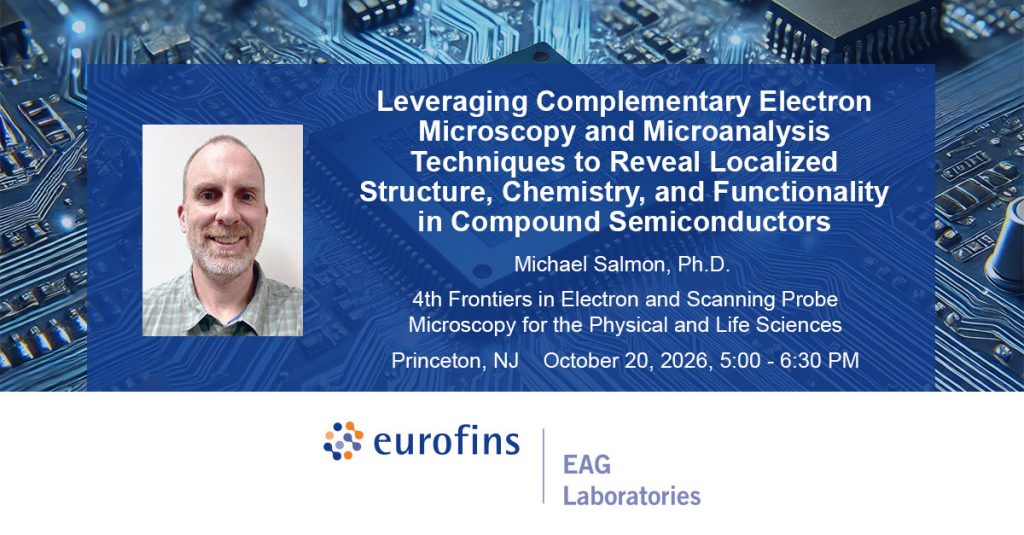
Leveraging Complementary Electron Microscopy and Microanalysis Techniques to Reveal Localized Structure, Chemistry, and Functionality in Compound Semiconductors

October 19 - 21, 2026

We are excited to announce that Eurofins EAG Laboratories will be presenting a poster at 4th Frontiers in Electron and Scanning Probe Microscopy for the Physical and Life Sciences in Princeton, NJ.

Meet Dr. Michael Salmon as he presents his poster on Tuesday, October 20th from 5:00 – 6:30 PM at the Princeton Friend Center.

Leveraging Complementary Electron Microscopy and Microanalysis Techniques
to Reveal Localized Structure, Chemistry, and Functionality in Compound Semiconductors

Electron–specimen interactions generate a rich variety of signals that provide complementary insight into a material’s structure, chemistry, and functionality. As a result, modern electron microscopy has evolved beyond imaging alone into a multimodal characterization platform capable of probing atomic-scale structure, local composition, optical behavior, and electronic functionality across multiple length scales. When combined with advanced microanalytical techniques and computational data analytics, these approaches enable a more complete understanding of complex semiconductor systems than can be achieved through any individual method alone.

This work highlights correlative characterization workflows developed for compound semiconductor materials and devices. Functional- and defect-sensitive imaging modalities are first employed to identify localized regions of interest associated with optical, electrical, and structural anomalies. Site-specific specimen preparation via focused ion beam (FIB) techniques subsequently enables targeted nanoscale and atomic-scale characterization, while complementary microanalytical methods, such as APT, provide quantitative compositional information and three-dimensional chemical mapping. Advanced computational analysis of electron microscopy datasets further expands these capabilities by revealing subtle structural features, improving measurement repeatability, and enabling statistically robust evaluation of complex microstructures. Through the correlation of these datasets, direct relationships can be established among local functionality, crystal structure, defects, bonding, dopant distributions, and impurity incorporation.

Representative examples include investigations of impurity segregation in FACELO AlGaN/GaN epitaxial structures, dopant diffusion along individual dislocations, polarity inversion in N-polar AlN associated with oxygen incorporation, failure analysis of GaAs-based VCSEL devices, and structure–function correlations in light-emitting device architectures. Together, these studies demonstrate how targeted, multimodal characterization workflows spanning multiple length scales and sensitivity regimes can uncover materials insights that are inaccessible through individual characterization techniques alone. Beyond advancing scientific understanding, these approaches provide practical solutions to real-world characterization challenges encountered in semiconductor research, process development, failure analysis, and manufacturing.

More content you might like...

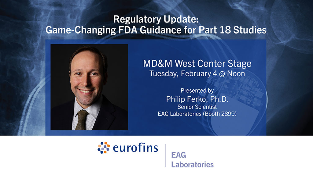
MD&M West 2025

February 4-6, 2025
Eurofins EAG Laboratories will exhibit and present at MD&M West in Anaheim. Dr. Philip Ferko, Senior Scientist with EAG, will present in the MD&M West Center Stage at 12pm on February 4.

Read More »

TEM

To enable certain features and improve your experience with us, this site stores cookies on your computer. Please click Continue to provide your authorization and permanently remove this message.

To find out more, please see our privacy policy.