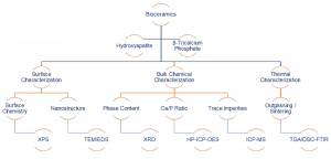
Characterization of Bioceramics for Surgical Implants: Part I – Precursor Qualification
This paper will demonstrate how analytical tools can be used for the quality control of hydroxyapatite and β-tricalcium phosphate powders

This paper will demonstrate how analytical tools can be used for the quality control of hydroxyapatite and β-tricalcium phosphate powders
Metallurgical testing lab services from EAG Laboratories includes grain size analysis, Rockwell hardness and image analysis.
Eurofins EAG has a wide array of analytical techniques to verify the cleanliness of medical devices. We’ve helped our customers evaluate the cleanliness of their products using techniques including NVR analysis, often in combination with FTIR, XPS and TOF-SIMS.

Eurofins EAG Laboratories is your partner for battery materials testing throughout the battery life cycle. From raw materials to product failures, we can provide the data needed to help you provide top quality and high-performance products to market faster.
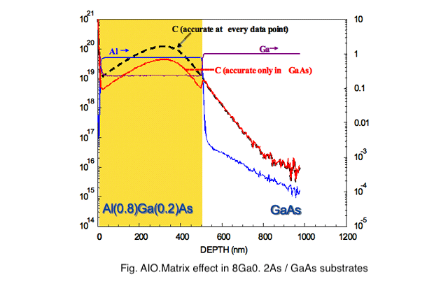
Compound semiconductor films are grown with different matrix compositions that affect the elemental sensitivities and sputtering rates
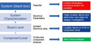
Electronic systems failure analysis methodology and workflow by applying FIB circuit edit techniques for solving electronic problems.
To enable certain features and improve your experience with us, this site stores cookies on your computer. Please click Continue to provide your authorization and permanently remove this message.
To find out more, please see our privacy policy.