EAG Extends Leadership in Electronics Failure Analysis Services with Millions in New Tool Investments

Evans Analytical Group (EAG), the world’s leading, fully integrated, independent laboratory network providing high value expert analytical and testing services to a wide range of industries and end users, today announced it has significantly enhanced its capabilities with the acquisition of multiple advanced imaging and inspection tools for electronics failure analysis. The new equipment extends EAG’s leadership position while enabling the company to better serve its customers with maximum speed, accuracy and effectiveness.

“This major investment further strengthens our ability to deliver best-in-class services to our customers, while reinforcing our position as one of the few providers with the necessary, highly specialized tools and expertise to localize electrical failures,” said Aram Sarkissian, general manager, Microelectronics Test and Engineering (MTE) for EAG. “We continue to be one of the best-equipped labs in the world for diagnosing and resolving a broad range of challenging IC and microelectronics failures.”

ATE Services from EAG Laboratories

Company Adds Latest Precision Imaging and Inspection Equipment to One of Industry’s Broadest Portfolios of Advanced Diagnostic Tools

Today’s advanced semiconductor technology nodes allow ICs to shrink in size while growing in complexity, which means even a single misplaced atom can lead to performance problems and difficult-to-diagnose failures. This requires the latest tools and equipment to keep up with technology advancements. EAG’s newest tool investments include the following acquisitions:

PHEMOS-1000 emission microscope from Hamamatsu Photonics K.K.: By detecting faint emissions caused by device anomalies, this microscope enables operators to identify failure locations in anything from memory and logic devices to power and flat panel devices. The tool offers superior detection, higher-resolution backside images, and lower detection thresholds than alternative tools while also providing laser marking to more easily transfer failure location information to another analytical instrument.

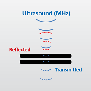
Scanning acoustic microscopy (SAM) icon from EAG Laboratories

OKOS VUE 400-P Scanning Acoustic Microscopy (SAM) and ultrasonic non-destructive package testing tool: This tool provides advanced imaging capabilities in conjunction with other visual examination methods. It uses ultrasound waves to detect changes in a materials’ acoustic impedances that, in a package failure, would reveal voids, delamination, or underfill problems. Available with multiple transducer options to support numerous package types, the tool can acquire multiple gates simultaneously for convenient single-scan capture of die surface, die attach and transmission mode (also known as thru-scan) images.

FA LIT layer-by-layer decapsulation tool from Control Laser: Patented laser technology enables EAG operators to systematically remove the individual layers of mold compound that typically cover a semiconductor die, all the way through the lead frames to the substrate. This improves decapsulation success rate especially in devices featuring copper wire, allows inspection of stitch bonds, and enables PCB trace probing or reworking.

EAG is the only company to focus its failure analysis services on the entire system, from electronics to materials and all the way down to IC transistor-level failure mechanisms. Its multi-disciplinary services include both materials characterization and electrical testing using the latest high-resolution microscopy imaging and electrical localization tools, and are delivered through a well-defined, holistic methodology that is customized for each customer situation. These capabilities are increasingly important given the growing complexity of electronics systems, their rapid pace of miniaturization, the special characteristics of advanced technology processes, the intermittent nature of system malfunctions, and difficult challenges posted by exotic materials that are used to design and manufacture today’s components.

About Evans Analytical Group

EAG is the world’s leading, fully integrated, independent laboratory network. EAG’s Materials Characterization Division provides high value analytical services focused on surface analysis and materials characterization in support of high technology industries. The Company’s Microelectronic Test and Engineering division provides expert engineering service and testing services for early engineering and new product introduction in support of the electronics industry. EAG’s ChemEco division provides analytical chemistry, environmental fate, metabolism and eco-toxicology services for agrochemicals, industrial chemicals, pharmaceuticals and animal health products. EAG has an international network of laboratories and serves more than 5,500 customers worldwide. (www.eag.com)

More content you might like...

ANTEC 2024

ANTEC 2024

March 4-7, 2024
Eurofins EAG Laboratories will be presenting “Characterization of Mycelium Biocomposites Under Simulated Weathering Conditions“ on March 6th. We hope to see you there!

Read More »

To enable certain features and improve your experience with us, this site stores cookies on your computer. Please click Continue to provide your authorization and permanently remove this message.

To find out more, please see our privacy policy.