
Meeting Material Purity Requirements with GDMS
Unwanted chemical impurities can be problematic. GDMS is a powerful full survey analysis tool for chemical purity evaluations.
Unwanted chemical impurities can be problematic. GDMS is a powerful full survey analysis tool for chemical purity evaluations.
April 2025
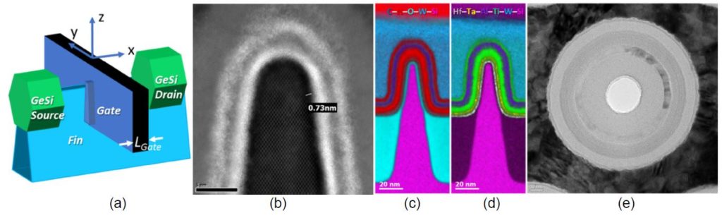
Curtis Ritter published and presented a paper, Using Thermal Reflectance Analysis with Microsanj for Open Defect Localization, in the 2025 IEEE International Reliability Physics Symposium (IRPS).
15th September 2023
EAG Laboratories is pleased to announce a new addition to our wide range of Advanced Microscopy techniques. We now offer Plasma FIB (PFIB) services!
EAG has established product reliability test processes. In this example we inspect a Bluetooth speaker using Accelerated Testing.
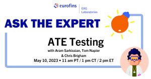
ATE testing automates and streamlines the testing process of microelectronic devices by using specialized hardware and software to perform a wide range of functional tests under various conditions. Come learn more about ATE and what EAG can do for you.
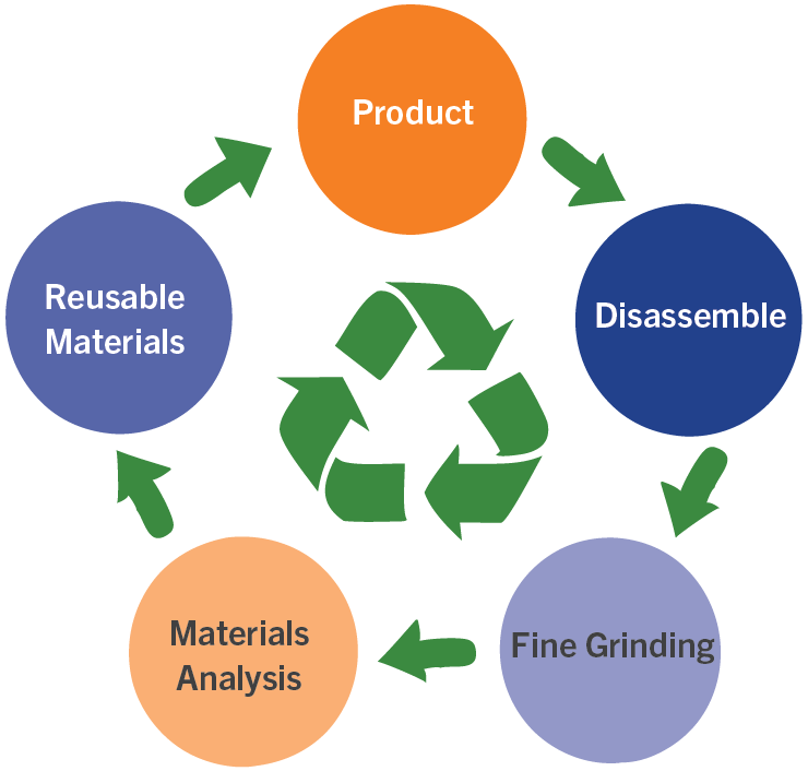
Recycling supports green technologies like electric cars and solar panels, protects the environment, and fits into Europe’s plan to reduce waste and use resources more sustainably.
To enable certain features and improve your experience with us, this site stores cookies on your computer. Please click Continue to provide your authorization and permanently remove this message.
To find out more, please see our privacy policy.