Continuous scaling of transistors below 5 and 3 nm technology nodes requires both novel device structure and materials that constitute the gate dielectrics and gate metal. With current technology nodes at 5 nm, GAA (gate all around) stack made up of nanosheets have been proposed as one of the alternate solutions [1-3] that can continue to provide the required drive current for on/off state for each transistor and do not suffer from leakage associated with the common contact at the bottom of the device, as in current finFET (field effect transistor) devices.
GAA transistors face their own engineering challenges, in fabricating the complex silicon nanosheet structure, with a Si-SiGe (silicon – silicon germanium) superlattice as the base stack. Moreover, as with each technology node, alternate materials for the gate metal/dielectric are also explored to optimize both performance and reduce power consumption. As this technology progresses there is a need to understand [a] uniformity of the nanosheets both in depth (z- direction) and lateral (x-y direction) more commonly known as line edge roughness, [b] dopant distribution within the nanosheets and [c] correlation between electrical performance metrics and processing impurities and contaminants at low concentrations (less than 100 ppm), typically low Z (atomic number) elements introduced during processing, such as C, O, N, F.
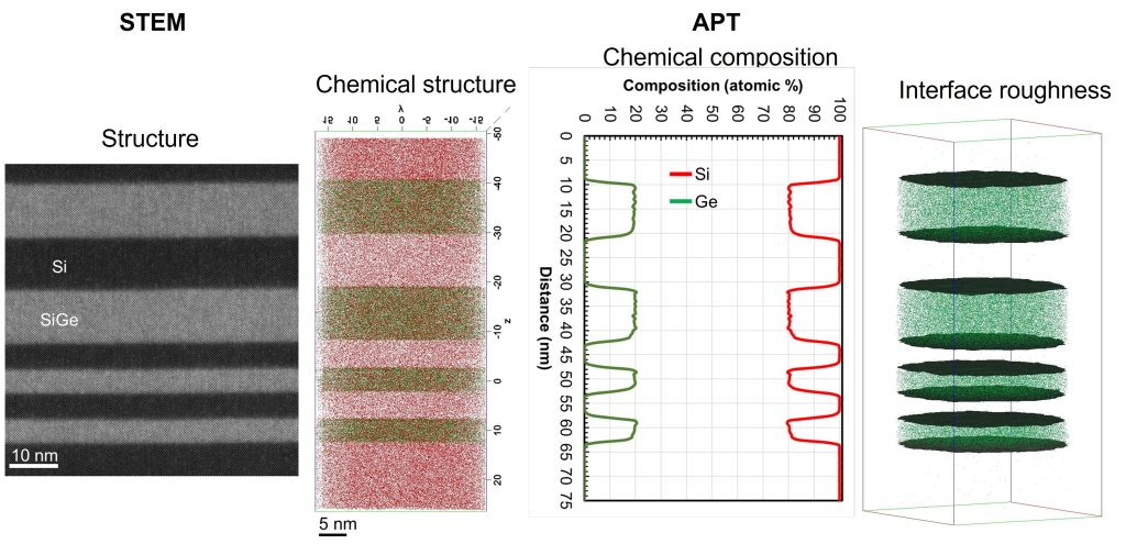
While current metrology such as STEM (scanning transmission electron microscopy) can provide high resolution structural information in 2D (two dimensional) and can help address uniformity in depth direction, projection issues from the thickness of the lamella being investigated and low chemical sensitive until ~ 1 at% prevent its usefulness in understanding dopant levels and impurities/contaminants for complex devices such as GAA. Other techniques such as nano SIMS (secondary ion mass spectrometry), SEM (scanning electron microscopy), AFM/SPM (atomic force microscopy, scanning probe microscopy), SAXS (scattering angle x-ray spectroscopy) also fail to provide the required spatial, depth or chemical resolution to observe and analyze individual GAA transistors [3,4]. As the development of this technology continues, there is a requirement for a metrology solution that can analyze from bulk films down to prepared devices and continue to do so for future smaller and/or shorter GAA transistors.
APT (Atom Probe Tomography), is one such metrology technique that provides both high spatial and chemical resolution in 3D. The ability to obtain ppm level element distribution in 3D, analysis of most elements on the periodic table and the ability to differentiate isotopes for a more accurate analysis, all satisfy the requirements for the semiconductor industry. In this work, using a blanket film with a tri layer of Si-SiGe superlattice, we perform chemical analysis that helps to resolve [a] uniformity of the layers in x, y and z direction, [b] depth analysis of dopants and identification of dopant present and [c] presence/absence of processing impurities within the superlattice. Our results indicate that P (phosphorous) with a concentration of 2E18 atoms/cm3 is doped uniformly in the superlattice and the films have good uniformity in the lateral direction, however analysis of interfaces in the z- direction reveal that Ge extends ~ 1nm into the Si layer.
Such a detailed chemical and 3D spatial analysis with APT, helps to address the shortcomings of other techniques in order to better characterize such films and subsequent devices thereof. Overall, APT enables a true 3D representation for the materials involved will help to accelerate the development of next generation semiconductor devices. With new tool developments and a strong focus on high throughput analysis, APT as a technique is slowly emerging as a viable solution to analyze current and future semiconductor devices, both 2D and 3D films and devices.
[1] D. Nagy, G. Indalecio, A. J. GarcíA-Loureiro, M. A. Elmessary, K. Kalna and N. Seoane, “FinFET Versus Gate-All-Around Nanowire FET: Performance, Scaling, and Variability,” in IEEE Journal of the Electron Devices Society, vol. 6, pp. 332-340, 2018, doi: 10.1109/JEDS.2018.2804383.
[2] N. Loubet et al., “Stacked nanosheet gate-all-around transistor to enable scaling beyond FinFET,” 2017 Symposium on VLSI Technology, 2017, pp. T230-T231, doi: 10.23919/VLSIT.2017.7998183.
[3] U. K. Das and T. K. Bhattacharyya, “Opportunities in Device Scaling for 3-nm Node and Beyond: FinFET Versus GAA-FET Versus UFET,” in IEEE Transactions on Electron Devices, vol. 67, no. 6, pp. 2633-2638, June 2020, doi: 10.1109/TED.2020.2987139.
[4] V. Pott, K. E. Moselund, D. Bouvet, L. De Michielis and A. M. Ionescu, “Fabrication and Characterization of Gate-All-Around Silicon Nanowires on Bulk Silicon,” in IEEE Transactions on Nanotechnology, vol. 7, no. 6, pp. 733-744, Nov. 2008, doi: 10.1109/TNANO.2008.2007215.
[5] N. G. Orji, et al., Metrology for the next generation of semiconductor devices, Nature Electronics 1 (10), 532-547 (2018). https://doi.org/10.1038/s41928-018-0150-9