Focused Ion Beam (FIB) Circuit Edit Becomes Increasingly Valuable in High-Stakes World of Advanced Node Design
Home » Focused Ion Beam (FIB) Circuit Edit Becomes Increasingly Valuable in High-Stakes World of Advanced Node Design
Integrated circuit (IC) designers are learning that a technique long used on older process nodes is providing even more valuable benefits as they develop devices to be manufactured at advanced technology nodes including 28nm and beyond.
During a period when it takes $10 million or more to bring a device to market, focused ion beam (FIB) circuit edit has become strategically important tool for reducing costs, optimizing performance and functionality, mitigating risk, and speeding time to market for complex device designs.
It is widely understood that IC designers will encounter many new problems at advanced process nodes that would be difficult, if not impossible, to anticipate based on previous design work. EDA tool providers are already addressing the difficulty of advanced node design with advice around design flow and other ways to handle numerous technical challenges.
In addition to applying these new design flow modifications, developers can also apply FIB circuit editing to the process of debugging and validating fixes or exploring design optimization changes, before committing to the high cost or lengthy timetables of a full mask spin.
TACKLING CHALLENGES AT ADVANCED PROCESS NODES
Design success barriers are magnified at advanced process nodes, where mask costs are high and it is much more difficult to find and fix bugs. It is widely understood that designers will encounter many new problems at advanced process nodes that would be difficult, if not impossible, to anticipate based on previous design work. The feature sizes of chips manufactured at 20nm process nodes are 10 times smaller than the wavelength of the laser light typically used in lithography. Pre-silicon testing is growing extremely tedious, simulation times are growing excessive, and many designs simply cannot be 100 percent verified. Simulation models may be imperfect for extremely complex designs, and packaging can cause stresses to sensitive devices.
Challenges in this environment range from multiple patterning and layout dependent effects (LDE) to the use of local interconnect layers. Design and integration complexity rises to a new level with each new technology node. Server signals and power electro-migration also create challenges. Decreasing metal pitch leads to coupling effects and signal integrity issues. Increasing wire and via resistance requires more advanced and variable wire sizing and tapering techniques. Additionally, extraction, timing, signal integrity analysis, and modeling pose a multitude of variation issues that designers must solve before they can achieve accuracy without compromising performance. Lithography limitations at 20nm often require a great deal of fixing to achieve signoff. Finally, designers face numerous chip and IP integration challenges, packaging issues, and additional complexity as these issues interact.
Similar challenges face designers of power control ICs and devices that combine control with power FET functionality. In these design environments, FIB circuit edit techniques similarly provide benefits at advanced process nodes, and will be increasingly important as many power devices move to silicon carbide (SiC), gallium nitride (GaN) and other wide bandgap materials.
Many EDA tool providers are already addressing these issues with advice around design flow and other ways to handle numerous technical challenges. This isn’t sufficient, however. In addition to applying new design flow modifications, developers can also apply FIB circuit editing with their early prototypes during de-bug. The same techniques can also be used to explore design optimization opportunities, by quickly and inexpensively implementing and creating physical prototypes that can be tested and validated before committing to the high cost or lengthy timetables of a full mask spin. FIB-edited device prototypes can be used to guide one-time modifications to masks, eliminating the need for a trial-and-error approach with successive versions of masks.
OVERVIEW OF FIB CIRCUIT EDIT CAPABILITIES
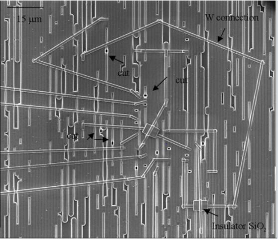
FIB systems have a number of uses in the semiconductor industry, microelectromechanical system fabrication, and biological studies. A primary use of FIB systems in the semiconductor industry is for circuit edit, allowing designers to cut traces or add metal connections within a chip (see Fig. 1). FIB edits can be performed quickly and easily, at a small fraction of the $5 million to $10 million in costs that are typical for a new lot of wafers in a fab. Using today’s state-of-the-art equipment, it is possible to edit circuits fabricated with 28 nm and smaller technology nodes that feature multiple-layer metal stacks and occupy flip chip and other advanced chip scale form factors.
FIB circuit edit is performed using a finely focused gallium (Ga+) ion beam with nanoscale resolution. It is possible to image, etch and deposit materials on an IC with an extremely high level of precision. By removing and depositing materials, FIB circuit edit enables designers to cut and connect circuitry within the live device, and to create probe points for electrical test.
It is the equivalent of performing microsurgery on IC devices. The high-energy Ga+ beam can mill through conductors, and uses various types of gases to either enhance milling precision or more effectively deposit conductive and dielectric materials). For instance, by using appropriate gas chemistries, a choice of tungsten, platinum or silicon dioxide can be very precisely deposited using the ion beam.
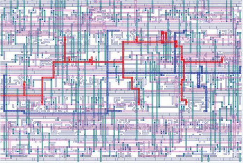
In order to perform circuit edits, the FIB tool is coupled to a CAD navigation system that makes it possible to locate the area of interest. FIB circuit edit typically uses the designer’s GDS files to navigate to the precise area. This provides a method to find subsurface features and ensuring that the right edits are made (see Fig. 2). Accurate beam positioning beam is one of the most critical requirements for FIB circuit edit.
FIB CIRCUIT EDIT APPLICATIONS
There are many uses for FIB circuit edit at every commercially available node. It can be used both to verify design change on the tester, and to validate design change at the system board level. Typical applications include:
- Debugging and optimizing devices that are already in production – FIB circuit edits are often performed once a design flaw has been identified. This ensures that the proposed fix will completely resolve the problem. Designers can repair mask errors and know that the device will work after one and not two mask spins, while simultaneously expediting the next steps by getting working prototypes into customers’ hands so they can continue software development. As cycle times in mobile device and other market segments become more and more compressed, avoiding a week of lost cycle time can be extremely important for a successful product roll-out.
- Exploring and validating design changes – more than just simulation that is required to optimize designs. FIB circuit edit goes beyond to the ultimate in emulation capabilities. It enables designers to try derivatives of device designs and observe the results. They can explore options like cut-away fuses or other functional changes, and experiment with them on a live device before committing to the cost or timetable of a complex mask spin.
- Prototyping new devices without costly and time-consuming mask set fabrication – FIB prototype devices are often used to enable next-level testing. This enables developers to get a jumpstart on the next round of device debug and accelerate design cycles. FIB circuit edit eliminates the need for multiple prototype testing rounds and mask modification cycles. Designers can implement and evaluate the results of circuit changes on physical prototypes that will optimize or correct flaws in the design before committing to them in a new mask spin. What would otherwise cost $5 million to $10 million in wafer costs and 6-8 weeks in wafer processing cycle time can be done for hundreds or thousands of dollars in a matter hours, ensuring that only one additional wafer spin will be required.
- Duplicating and scaling fixes: Once a fix has been verified on a prototype using FIB circuit edit, it is possible to duplicate that fix on handful or tens of devices to provide internal test, validation, and qualification teams and even customer samples. By doing this, further system or application development work can then take place in parallel while waiting for the mask spin and final production devices to come back.
- Accelerating time to market: Delivering on time is vitally important to customers. Their product designs are essentially on hold until they can get devices. FIB circuit edit speeds up the entire cycle. It gets customers into production and avoids loss of reputation, or the risk of competitors getting their foot in the door, etc. Some large OEM customers also impose late-delivery penalties that can sometimes reach millions of dollars.
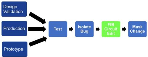
Fig. 3 shows the best approach for integrating FIB circuit edit into the overall IC development and testing process.
In the power semiconductor arena, most current control products are fabricated using traditional silicon technology, and FIB circuit edit is performed in much the same way with these devices as it is with any other analog or digital circuit. In the future, there is a strong possibility that drivers will move to wide bandgap materials. FIB circuit edit should offer benefits for these devices, as well. SiC, GaN and other wide bandgap semiconductor materials enable power semiconductor devices to withstand high voltages and temperatures, while providing higher frequency response, increased current density and faster switching speeds.
At the same time, however, they present complex challenges related to design and characterization, process monitoring and reliability. Challenges become even more difficult at advanced process nodes.
FIB CIRCUIT EDIT TECHNIQUES CONTINUE TO IMPROVE
There is a relatively common misperception that FIB circuit edit only works well at 90nm and 65nm process nodes, and that it has “run out of gas” at anything below. This is simply not true. Thanks to tool and methodology advances that have been derived from the experience of dedicated teams running thousands of circuit edit hours/months, FIB circuit edit can now be used for more precise beam guidance, operate in smaller areas, perform more intricate operations on both the back and front sides of the device, and handle copper layers.
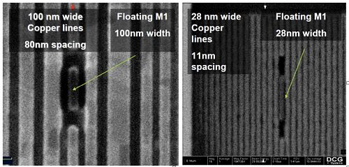
A major development area for FIB circuit edit is the ability for tools to provide better aspect ratio for smaller cuts as part of the solution. FIB systems continue deliver greater benefits thanks to advances in areas such as ion beam resolution, operating software and CAD navigation. Ion beam resolution advances, alone, have delivered significant new capabilities that have been critical for recognizing small features, aiding in visual end-pointing, enabling precise CAD alignment, and improving box placement accuracy.
Fig. 4 shows resolution advances that have been achieved from 2008 to the present.
Tool advances are only part of the story, however. Because FIB tools are not entirely automated, there is no under-estimating the critical importance of FIB operator experience to circuit edit success.
For example, endpoint detection, or the ability to know when selected layers of interest have been successfully etched) continues to require a high level of skill in order to achieve high success rates. Operator skill in this area is even more important at smaller geometries, and during particularly challenging FIB operations. Also important is the unique operator knowledge in such areas as IC circuitry, IC process technology, ion milling patterns, and general FIB tool usage basics.
Achieving this expertise can be difficult for an in-house operation. Often, larger semiconductor companies who already conduct some level of circuit edit will augment these resources with external service labs that have deeper and more extensive experience in solving the toughest FIB circuit edit challenges. As for small- and mid-sized companies, few can bear the expense of purchasing a FIB tool that might cost $1 million or more. Even if they could afford the tool, it would be difficult to staff a team with the necessary experience to most effectively operate it. Most companies of this size tend to go directly to an external lab that can implement circuit edits to support basic electrical design characterization or verification of redesign parameter, and offers a full range of debug tools necessary for solving difficult logic failures and other anomalies.
BEST PRACTICES FOR FIB CIRCUIT EDIT
There are numerous prerequisites for FIB circuit edit success, including:
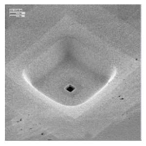
- Tools: High resolution is particularly important at advanced nodes such as 28nm and 20nm. Designs generally require a .1um resolution (or aspect) ratio as well as a trenching approach that supports a finer resolution in order to make these edits. The smallest hole that can be made with today’s equipment is 0.1×0.1um with an aspect ratio of 1/20. For most 20nm and 28nm designs, it is impossible to make a small enough hole to reach the target. As a result, specialized FIB techniques are required in order to lower the aspect ratio and gain access to the target. The system must be able to smoothly remove dummy metal above the target metal layer. This also requires deep and extensive knowledge of IC circuitry and processes, FIB tools and ion milling patterns. Figure 5 shows a typical back-side trench.
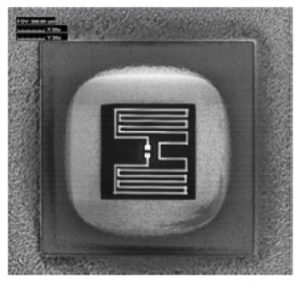
- Backside and frontside editing: Many erroneously believe that flipchip FIB circuit edit can only be performed from the top of the device, and that neither backside or frontside editing are possible. On the contrary, backside edit is frequently the most effective way to operate. This might be true because of substrate material in flipchip packaging, or because of the increased number of metal circuit layers in today’s ICs, which makes it harder to reach a lower layer when editing from the top. Fig. 6 shows a back-side FIB circuit edit in which a resistor is introduced across two nodes.
In another example, Fig. 7 shows a typical back-side FIB circuit edit in which a probe pad is formed for micro probing.
- Handling copper layers: Most 28nm and 20nm devices are copper devices that feature a crystal structure which is very difficult to remove smoothly. Special methods are required, as well as the engineer’s experience so that the metal can be removed smoothly with a very high level of quality. Also, accurate beam positioning is more challenging for copper metal devices due to the non-visibility of the circuit patterns. This is also important for aluminum metal devices if there are no unique patterns to recognize on the top level.
- Companion failure analysis and test tools, expertise and capabilities: Because most devices must ultimately find their way into packages, there should be a smooth transition to de-capping or de-lidding the devices and performing micro-probing and other de-bugging tests on FIB-edited parts.
- Front-end expertise: In addition to presenting challenges due to ever-shrinking nano-scale geometrics, semiconductor advanced technology nodes also introduce new front-end materials as processes evolve. FIB circuit edit labs can benefit from being part of a larger lab environment characterized by a significant level of front-end process understanding and materials expertise. Labs that support process R&D activity and yield support will be abel to offer an advantage and insights, as well as other know-how that will help maximize the success of FIB circuit edit strategies.
GROWING IN VALUE
IC design verification and validation will continue to increase in difficulty as the industry moves down the nano-scale geometry curve. While some may believe that FIB circuit edit is
![Figure 7 High-resolution trenching enables edits at advanced nodes. [Image courtesy of FIB International Inc.]](https://www.eag.com/wp-content/uploads/2016/10/white-paper-focused-ion-beam-fib-circuit-edit-becomes-increasingly-valuable-in-high-stakes-world-of-advanced-node-design-M-001416_Figure_7-300x285.jpg)
obsolete at today’s advanced nodes, it is actually becoming increasingly valuable for improving the success rates for these designs, which often can cost $10 million or more to bring to market. Due to advances in both tool technology and best practices, FIB circuit edit can be used at advanced nodes for a variety of purposes including debugging and validating fixes, as well as earlier in the process to explore opportunities for design optimization, without having to commit to an expensive and time-consuming full mask spin.
Would you like to learn more about Focused Ion Beam (FIB) Circuit Edit ?
Contact us today for your Focused Ion Beam (FIB) Circuit Edit needs. Please complete the form below to have an EAG expert contact you.