
More Than Testing – Your One Stop Shop
Developing a reliable product has many challenges due to the desire for increased capability, reduction in formfactor, and managing the supply chain.

Developing a reliable product has many challenges due to the desire for increased capability, reduction in formfactor, and managing the supply chain.
In this webinar we introduce Metal Based Additive Manufacturing Analysis to understand and evaluate many aspects of the metallurgy.
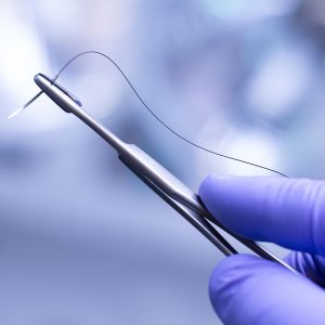
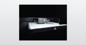
Cold stage analysis has been shown to be effective for samples that are not solids at room temperature or that have components that are volatile in a vacuum system, such as the antibacterial coated sutures.

X-ray diffraction (XRD) is a powerful and versatile technique that can give detailed structural information about almost anything that is solid.
To enable certain features and improve your experience with us, this site stores cookies on your computer. Please click Continue to provide your authorization and permanently remove this message.
To find out more, please see our privacy policy.