Thin Film Analysis Webinar
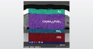
In the full webinar we will discuss Thin Film Analysis that looks at film composition, thickness, and uniformity.
In the full webinar we will discuss Thin Film Analysis that looks at film composition, thickness, and uniformity.

Rare earth magnets power some of today’s most advanced technologies. Part 3 of this series explores how the magnets are produced, challenges of maintaining purity at every step, and why precision analysis is essential for building a reliable supply chain.

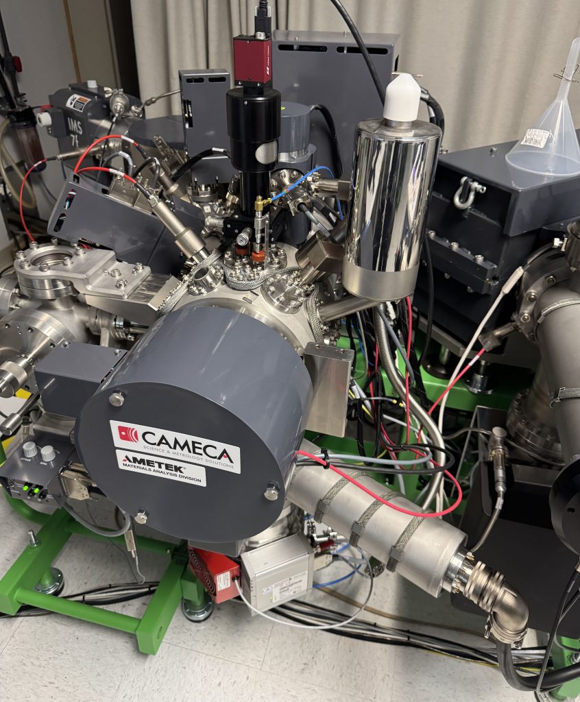
APT is a nanoscale materials analysis technique that provides 3D spatial imaging and chemical composition measurements with high sensitivity simultaneously.
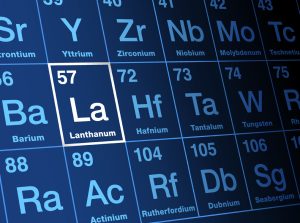
The term ‘rare earth elements’ (REEs) is a misnomer and better refers to the relatively rare ores REEs are extracted from; rare earth elements are all around us!
To enable certain features and improve your experience with us, this site stores cookies on your computer. Please click Continue to provide your authorization and permanently remove this message.
To find out more, please see our privacy policy.