TXRF Webinar
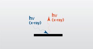
In this webinar we introduce Total Reflection X-ray Fluorescence (TXRF) which is a non-destructive elemental survey technique.
In this webinar we introduce Total Reflection X-ray Fluorescence (TXRF) which is a non-destructive elemental survey technique.

EAG Scientists utilize GDMS analysis to perform Elemental Depth Profiling for chemical purity evaluations for aerospace & defense.
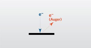
This webinar is an introduction to Auger Electron Spectroscopy. It will include the principles of the technique with examples.
This webinar covers FDA regulation of medical devices, the most commonly used test standards, and custom testing at Eurofins EAG Laboratories.
To enable certain features and improve your experience with us, this site stores cookies on your computer. Please click Continue to provide your authorization and permanently remove this message.
To find out more, please see our privacy policy.