Extractable & Leachable Studies for Consumer Products Webinar
In this webinar we introduce Extractable and Leachable tests which identify chemical components that can migrate out of a product.

In this webinar we introduce Extractable and Leachable tests which identify chemical components that can migrate out of a product.
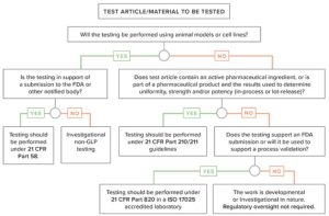
Medical device regulations are not entirely clear, EAG shows the decision process for contract analytical laboratories to support development.
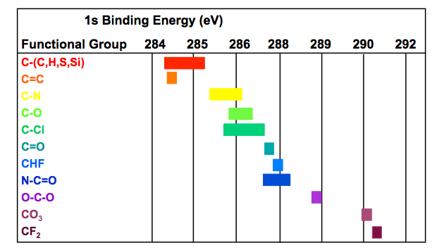
XPS shows the species present can be determined or estimated from the measured chemical shift of the binding energy of each element
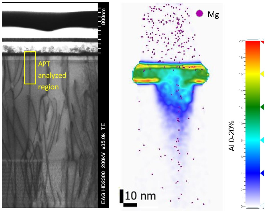
Auger Electron Spectroscopy (AES) is effective in determining the quality of passivation layers to prevent corrosion in medical devices.

This webinar will focus on Electron Backscatter Diffraction (EBSD) and Electron channeling contrast imaging (ECCI)
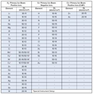
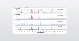
SIMS analytical technique typical detection limits for impurities in a HgCdTe matrix for normal depth profiling conditions.
To enable certain features and improve your experience with us, this site stores cookies on your computer. Please click Continue to provide your authorization and permanently remove this message.
To find out more, please see our privacy policy.