Microscopy & Microanalysis 2026

Eurofins EAG to present at Microscopy & Microanalysis

August 2 - 6, 2026

We are excited to announce that Eurofins EAG Laboratories will be speaking at the Microscopy & Microanalysis (M&M) conference in Milwaukee, WI on Tuesday, August 4, 2026.

Correlative 4D-STEM, PED, and Spectroscopic Microscopy for Quantifying Ion-Induced
Structural Modifications in Si/SiGe Multilayer Architectures

Session: P03.3 Advanced TEM analysis for Semiconductors
Session Date & Time: Tuesday August 4, 2026, 10:30 AM – 12:00 PM
Presentation Time: 11:15 AM – 11:30 AM
Room: S102 E

Advanced Si/SiGe multilayer heterostructures used in gate-all-around (GAA) transistor technologies are highly sensitive to nanoscale processing-induced modifications. Accurate quantification of structural, strain, and compositional perturbations requires the integration of complementary electron microscopy modalities. Here, we establish a correlative, distance-resolved microscopy framework combining aberration-corrected STEM (AC-STEM), precession electron diffraction (PED), 4D-STEM nanodiffraction, and STEM-EDS/EELS to quantify ion-beam–induced modifications in Si/SiGe quantum well stacks.

To simulate dry etching processes used in semiconductor fabrication, Ga focused ion beam (FIB) and Xe plasma FIB were employed to etch the multilayer stacks under a thin metal capping layer. Atomic-resolution STEM imaging, coupled with advanced image analysis, enabled quantitative interface characterization as a function of distance from etched top surfaces and sidewalls.

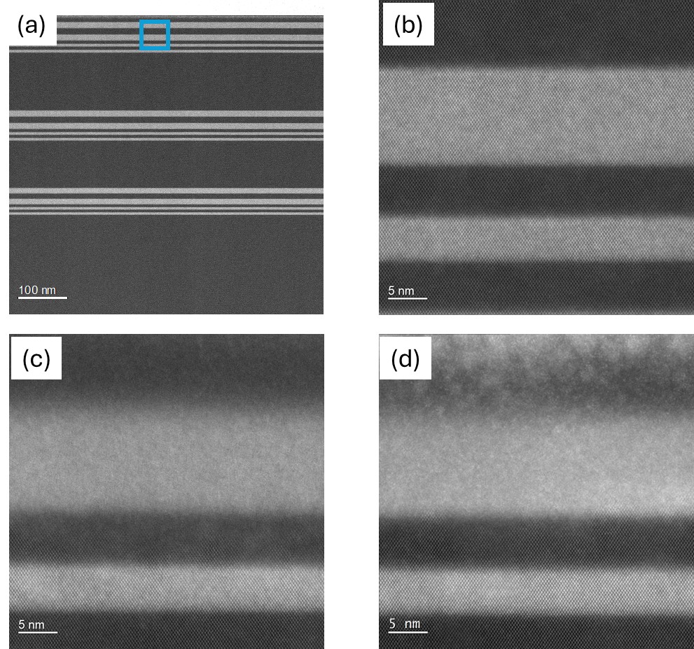
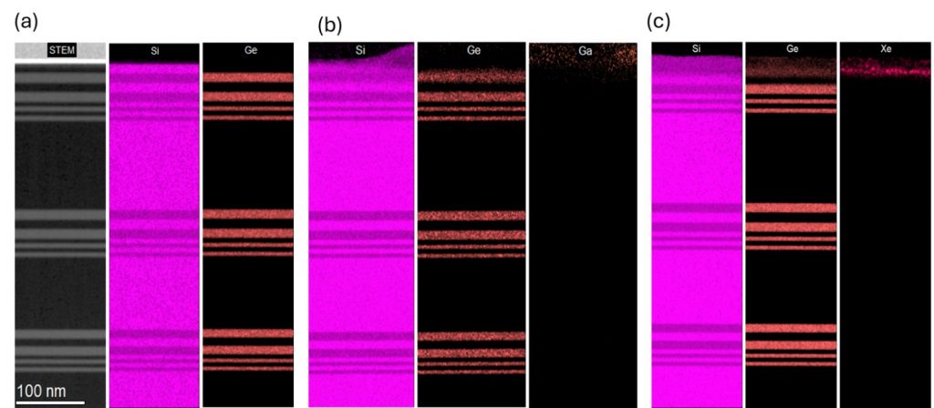
The Si/Ge multilayer structure consists of three groups of quantum wells. Following 30 kV ion etching, only the upper ~40 nm beneath the surface exhibited amorphization. In the Ga-etched sample, the first and second SiGe layer became fully amorphous, whereas the Xe-etched sample retained partial lattice crystallinity in the 2nd layer, indicating a shallower effective penetration depth for Xe compared to Ga ions (Figure 1). STEM-EDS mapping revealed Si and Ge redistribution after ion exposure (Figure 2). Notably, Xe was detected beneath the metal capping layer and accumulated within the first SiGe layer, in contrast to the Ga-etched sample. Interdiffusion of Si and Ge at the etched sidewalls was also observed.

HAADF of Si/SiGe stack (a) reference sample and (b) zoom in image, (c) from Ga-etched and (d) Xe-etched sample.

Figure 1. HAADF of Si/SiGe stack (a) reference sample and (b) zoom in image, (c) from Ga-etched and (d) Xe-etched sample.

HAADF and EDS map of (a) reference, (b) Ga-etched and (c) Xe-etched sample.

Figure 2. HAADF and EDS map of (a) reference, (b) Ga-etched and (c) Xe-etched sample.

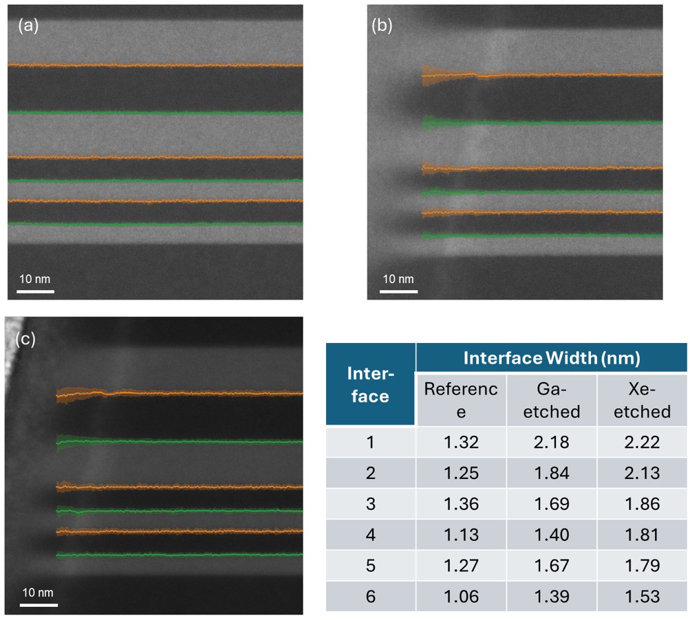
Using advanced image processing techniques, interface width was quantitatively extracted. Increased interface broadening was measured proximal to the ion-modified regions (Figure 3). The Xe-etched sample exhibited slightly greater interface widening compared to the Ga-etched sample, potentially associated with differences in beam profile and scattering characteristics.

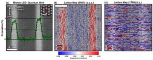
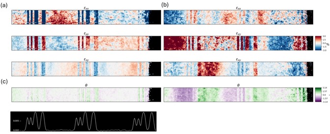
As shown in Figure 4, PED provided high-precision strain quantification across the multilayer heterostructure, revealing pronounced periodic tensile strain (εyy) along the [002] growth direction consistent with coherent Si/SiGe layering in the reference sample. In the Ga-etched sample, 4D-STEM strain mapping showed that this periodic modulation weakens and exhibits reduced periodic uniformity near the ion-impacted regions, accompanied by reduced diffraction contrast. In contrast, the Xe-etched sample retained more intact periodic strain away from the impacted surface, with disruption confined more locally, consistent with a more limited structural modification compared to Ga-etched sample.

Interface of Si/SiGe at the sidewall of sample of (a) reference, (b) Ga-etched and (c) Xe-etched. The table is the calculated width from the six interfaces inside the images.

Figure 3. Interface of Si/SiGe at the sidewall of sample of (a) reference, (b) Ga-etched and (c) Xe-etched. The table is the calculated width from the six interfaces inside the images.

Strain maps from 4D STEM data of (a) Ga-ion etched (b) Xe etched sample. (c) Strain yy profile measured by PED on reference sample.

Figure 4. Strain maps from 4D STEM data of (a) Ga-ion etched (b) Xe etched sample. (c) Strain eyy profile measured by PED on reference sample.

Future work will incorporate patterned, mask-defined etch geometries to more closely emulate GAA fabrication processes and systematically compare ion-species-dependent modification mechanisms. Monochromated EELS will be further employed to probe potential electronic structure changes induced by ion etching. This work establishes a quantitative correlative microscopy methodology for resolving nanoscale structural, strain, and compositional perturbations in advanced strained semiconductor architectures.

References:
[1] C. Ophus, Microscopy and Microanalysis (2019) 25, 563-582.
[2] M.G. Masteghin, et al., Small Methods (2026), e02258
[3] L. Li, et al., Electron (2024) 2, e32
[4] R. Ding, et al., J. Vac. Sci. Technol. A (2009) 27, 836-843

More content you might like...

Petalite

Battery Raw Material Testing

Battery Raw Materials Analysis Battery manufacturing is a meticulous process where the integrity and performance of the final product hinge on the purity of its raw materials. Contaminants, even in

Read More »

To enable certain features and improve your experience with us, this site stores cookies on your computer. Please click Continue to provide your authorization and permanently remove this message.

To find out more, please see our privacy policy.