Scanning Electron Microscopy (SEM)
Home » Our Techniques » Imaging » SEM
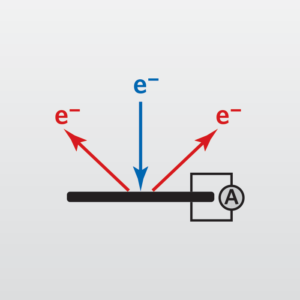
Scanning Electron Microscopy (SEM) provides high-resolution and high-depth-of-field images of the sample surface and near-surface. SEM is one of the most widely used analytical tools, due to the extremely detailed images it can quickly provide. Coupled to an auxiliary Energy Dispersive X-ray Spectroscopy (EDS) detector, SEM also offers elemental identification of nearly the entire periodic table.
EAG uses SEM analysis in cases where optical microscopy cannot provide sufficient image resolution or high enough magnification. The SEM also excels in producing detailed surface topography images. Applications include failure analysis, dimensional analysis, process characterization, reverse engineering and particle identification.
EAG’s expertise and range of experience is invaluable to the industries and customers we serve. Person-to-person service ensures good communication of the results and their implications. Customers are often present during the analysis, enabling an immediate sharing of data, imaging and information.
Ideal Uses of Scanning Electron Microscopy
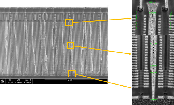
Scanning Electron Microscopy (SEM) is one of the most widely used analytical tools due to the extremely detailed images it can quickly provide. Combined with the capability of micro cleaver, it can offer sub nanometer resolution of cross section images with faster turnaround time.
- High-resolution surface topography images
- Elemental microanalysis and particle characterization
- Volume profile check before diving into advanced TEM/STEM imaging
- Medical device chemical characterization and equivalency testing via ISO 10993:19
Strengths
- Rapid, high-resolution imaging
- Quick identification of elements present
- Excellent depth of field (~100x that of optical microscopy)
- Versatile platform that supports many other analysis techniques
- Low vacuum mode enables imaging of insulating and hydrated samples
Limitations
- May need to etch planar samples for contrast
- Size restrictions may require cutting the sample
- Ultimate resolution is a strong function of the sample chemistry and stability in the electron beam
- If UHV surface analysis is required, it should be done first to avoid the possible introduction of surface carbon by the SEM
Scanning Electron Microscopy Technical Specifications
- Signals Detected: Secondary and backscattered electrons and X-rays, light (Cathodoluminescence) and Electron Beam Induced current (EBIC)
- Elements Detected: B-U (EDS mode)
- Detection Limits: 0.1-1 at%
- EDS Chemical depth resolution: 0.1-3 µm
- Imaging/Mapping: Yes
- Lateral Resolution/Probe Size: 10-30 Å
Related Resources
Why use Eurofins EAG for cross-section SEM?
EAG’s expertise and range of experience is invaluable to the industries and customers we serve.
- Fast turnaround time (<8 hrs)
- 24/7 support on large volume submission
- Precise micro cleaving on target larger than 5μm
- IP secured production control
- Years of experience with different materials and feature types
- Dedicated team to support your projects
- Improved efficiency to get better and faster results to you
- Compatible systems with sub nanometer resolution
- Seamlessly embedded in microscopy network
Would you like to learn more about using Scanning Electron Microscopy (SEM)?
Contact us today for your Scanning Electron Microscopy (SEM) needs. Please complete the form below to have an EAG expert contact you.