Atomic Force Microscopy (AFM)
Home » Our Techniques » Imaging » AFM
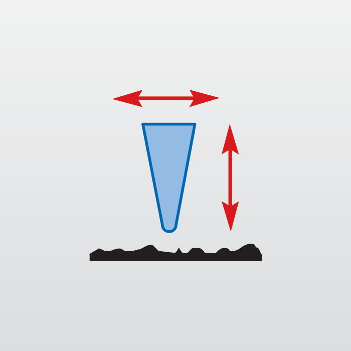
Atomic Force Microscopy (AFM) analysis provides images with near-atomic resolution for measuring surface topography. AFM is also referred to as Scanning probe microscopy. Atomic Force Microscopy is capable of quantifying surface roughness of samples down to the angstrom-scale. In addition to presenting a surface image, AFM analysis can also provide quantitative measurements of feature sizes, such as step heights and other dimensions. Additionally, advanced modes of atomic force microscopy measurements allow for the qualitative mapping of various other physical properties, such as adhesion, modulus, dopant distribution, conductivity, surface potential, electric field, and magnetic domains.
Contact Mode AFM
In contact mode AFM, the tip is scanned in contact with surface, and a Laser is reflected off the cantilever. The light position is detected on a photodiode. A constant position is maintained by adjusting the cantilever height with a voltage. The voltage is the output signal and relates to the topography.
Tapping Mode AFM
In tapping mode AFM the cantilever is oscillated. Forces between the tip and sample cause changes to the oscillation . A feedback loop maintains constant oscillation amplitude by adjusting tip height with a voltage applied to a piezo element. Applied voltage relates to topography with minimal damage to surface and tip. Tapping mode AFM is the common mode for topography imaging.
Ideal Uses of AFM
- Assessing wafers or thin films on wafers (e.g. SiO2, GaAs, SiGe, etc.) before and after processing
- Investigating processing effects (e.g. plasma treatment) on biomedical devices such as contact lenses, catheters and coated stents
- Examining the impact of surface roughness on adhesion
- Assessing trench shape/cleanliness on processed/patterned wafers
- Determining whether morphology is the source of surface hazes
- Mapping the distribution of activated carriers
- Characterizing the uniformity of thin conductive films
- Measuring step heights between domains on patterned wafers
- Three-dimensional surface topographic imaging, including surface roughness, grain size, step height, and pitch
- Imaging of other sample characteristics, including magnetic field, capacitance, and friction
- Phase imaging allows the investigation of physical characteristics of surfaces, such as modulus and adhesion
Strengths
- Firstly, quantifying surface roughness
- Secondly, wafers up to 300 mm can be analyzed intact
- Thirdly, high spatial resolution
- Lastly, imaging of conducting and insulating samples
Limitations
- Scan range limits: 90 µm laterally (xy) and 5 µm vertically in z-direction
- Potential problems with extremely rough or oddly shaped samples
- Tip-induced errors are possible
- Many electrical and magnetic modes are limited to qualitative or semi-quantitative measurements
AFM Technical Specifications
- Signal Detected: Topography
- Vertical Resolution: 0.1 Å
- Imaging/Mapping: Yes
- Lateral Resolution/Probe Size: 2-150 nm
- Advanced Analysis Modes:
- sMIM: Scanning Microwave Impedance Microscopy
- SCM: Scanning Capacitance Microscopy
- PFM: Piezo-Response Force Microscopy
- C-AFM: Conductive AFM
- TUNA: Tunneling AFM
- KPFM: Kelvin Probe Force Microscopy
- SSRM: Scanning Spreading Resistance Microscopy
- EFM: Electrostatic Force Microscopy
- MFM: Magnetic Force Microscopy
- PFQNM: Peak Force Quantitative Nanomechanical Microscopy
Would you like to learn more about using Atomic Force Microscopy (AFM)?
Contact us today for your Atomic Force Microscopy (AFM) needs. Please complete the form below to have an EAG expert contact you.