Atom Probe Tomography (APT)
Home » Our Techniques » Imaging » Atom Probe-3DAP/APT
Atom probe tomography (APT) is a nanoscale materials analysis technique that provides 3D (three-dimensional) spatial imaging and chemical composition measurements with high sensitivity.
The technique relies on ionization and subsequent field evaporation of individual atoms/atomic clusters from a specimen surface. The specimen is prepared in the form of a conical tip with an apex radius < 100 nm. The field evaporation occurs as a result of a base DC voltage bias (typically between 1-10 kV) and a pulsed voltage (conductive samples) or pulsed laser (semiconducting and insulating samples). The specimen is also cryogenically cooled down to between 25-80 K to suppress thermal lattice vibrations and improve on spatial positioning.
2D maps (Device level): These are used to provide information about the device structure and to correlate with other techniques.
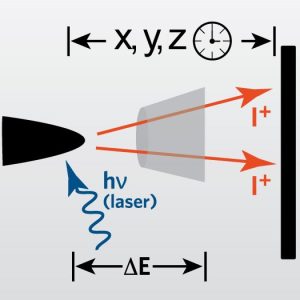
Field evaporated ions are collected onto a position sensitive detector (PSD) to accurately identify x and y position. The sequence of ions collected is used for z position. The x, y and z together provide the spatial imaging of the specimen tip. The time of flight of the ions is also measured and converted to a mass to charge ratio for chemical composition measurements. The spatial resolution is up to 0.3 nm in depth and 0.5 nm laterally, which is limited to metallic samples. The resolution for semiconducting and insulating samples is lower, typically ~ 1 nm at best. The chemical sensitivity for APT is 10 ppm.
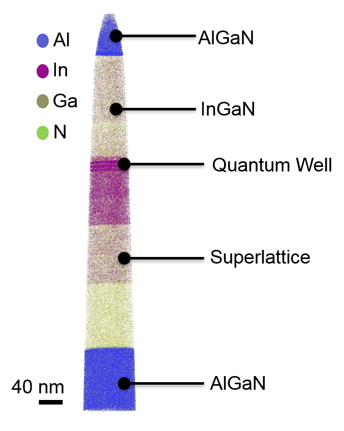
With analysis areas that are ~ 30-50 nm in x and y and between 100-500 nm in z based on material type, this technique is particularly useful for cases where [a] 3D structures/buried interfaces are present, [b] low atomic number (Z) elements are present, either as dopants or in the bulk and [c] nanometer sized clusters are part of the structure. While APT does not provide the same chemical sensitivity as SIMS (secondary ion mass spectrometry), it enables identification of elements within 3D structures that is not possible with SIMS. It also provides higher chemical sensitivity than TEM/STEM (scanning/ transmission electron microscopy) related techniques such as EDX (energy dispersive X-ray spectroscopy) and EELS (electron energy loss spectroscopy). 3D Compositional analysis of nanoscale clusters is routinely carried out using APT, as it is not possible to measure using TEM/STEM.
The LEAP 5000XR at Nanolab is currently the latest in the instrument capability with highest detector efficiency, higher signal to noise ratio and larger volumes captured and analyzed compared to older versions of the instrument. These enable capture of low concentration elements in 3D that are not possible to measure using other techniques.
Ideal Uses of Atom Probe Tomography (APT)
- 3D structure analysis such as FinFET, PMOS cap layer, 3D NAND, curved or non-uniform grain boundaries in photovoltaics.
- Nanoscale precipitates and matrix analysis for composition and chemical identification such as metallic alloys (Al 7075, shape memory, Ti).
- Light element analysis — Be, B, Li, C and Al, such as Li-ion batteries.
- Low concentration dopants in 2D and 3D for LEDs, finfets, 3D NAND memory and surface coatings of Li-ion batteries.
Types of Analysis
- Elemental maps: Observation of individual chemical species in the material/device for homogeneity/heterogeneity and 2D or 3D location is an important aspect of Atom Probe Tomography analysis. Typically 2D maps and 3D movies are used for this analysis.
- Compositional variation: APT provides multiples ways to analyze composition, such as line profile, proxigram and iso-concentration surfaces that are based on depth or concentration.
- Cluster analysis: APT has a strong suit in analysis for nanoscale (1-10 nm) clusters of elements within a matrix. The cluster size and composition for individual clusters of any shape and size can be analyzed with APT. With a large number of clusters, further quantitative analysis can be carried out.
- Dopant identification and composition: Identification of dopant location in 3D, its chemical composition and number density (until ~10 ppm or 5E18 atoms/cm3, in best cases) can be obtained using APT.
- Correlative study: In many cases, correlative studies with complementary techniques can help to answer our customer’s specific material questions. STEM, EBIC, EBSD, Electron tomography and SIMS are all techniques that are routinely used to aid the interpretation of 3D APT data.
- Specific region analysis: Based on customer requirements, a combination of different analysis can be used to better understand a specific region.
Atom Probe Tomography (APT) Strengths
- Small volume dopant mapping.
- Light element (e.g. Li and B) detection and mapping.
- Ability to identify isotopes.
- Equal probability of detection of all elements (H-U).
- Cluster analysis for nanoscale precipitates.
- High mass resolution to identify various elements present in the specimen.
APT Limitations
- Significant sample preparation time (4-6 hours).
- Small sampling volumes.
- Low data acquisition yield as some materials may not stable in the high electric field.
- Optimized parameters need to be obtained for each material type and structure.
- Low quantification accuracy for certain cases containing different elements with overlap in mass spectrum.
- Spatial resolution and composition accuracy can be limited for heterojunctions or complex geometries due to trajectory aberrations.
APT Technical Specifications
- Analysis type: 3D
- Material type: Metals, semiconductors, oxides, ceramics.
- Elements Detected: H-U
- Detection Limits: ~10 ppm (~ 5E18 atoms/cm3)
- Imaging/Mapping: Yes
- Maximum Lateral Resolution: 0.5 nm in lateral and 0.3 nm in depth
- Analysis area: 50*50 nm2
- Analysis Depth: 100-500 nm
- Detected Ion Type: Positive Charged
- Isotope identification: Yes
Would you like to learn more about using Atom Probe Tomography (APT)?
Contact us today for your Atom Probe Tomography (APT) needs. Please complete the form below to have an EAG expert contact you.