Ask the Expert: Residual Gas Analysis
RGA is ideally suited for process development, sealing quality control, studying long-term outgassing of the enclosed materials inside the components, and for product qualification.

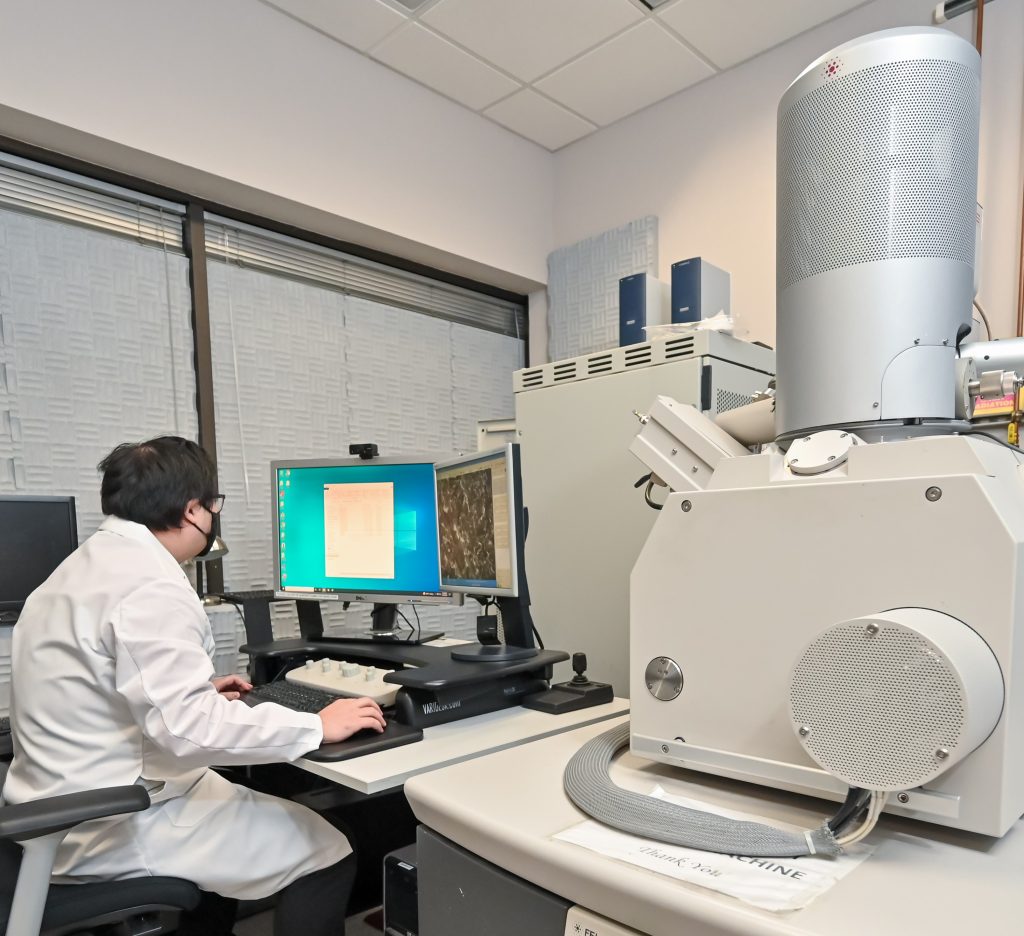
RGA is ideally suited for process development, sealing quality control, studying long-term outgassing of the enclosed materials inside the components, and for product qualification.

To be hermetically sealed essentially means to be airtight so that nothing can come in or get out (i.e., gas, moisture, liquid, etc.).
Unwanted chemical impurities can be problematic. GDMS is a powerful full survey analysis tool for chemical purity evaluations.
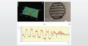
In the full webinar we will focus Full Survey Chemical Analysis of
Plasma Resistant Ceramic Coatings using GDMS
To enable certain features and improve your experience with us, this site stores cookies on your computer. Please click Continue to provide your authorization and permanently remove this message.
To find out more, please see our privacy policy.